Epitaxial wafer for flip infrared light-emitting diode

An infrared light-emitting and diode technology, applied in electrical components, circuits, semiconductor devices, etc., can solve the problems of difficult to obtain interface quality quantum wells and quantum barrier layers, and the brightness of light-emitting diodes cannot be effectively improved, so as to achieve the effect of improving quantum efficiency.

Inactive Publication Date: 2017-01-04
YANGZHOU CHANGELIGHT
View PDF6 Cites 14 Cited by
  • Summary
  • Abstract
  • Description
  • Claims
  • Application Information

AI Technical Summary

Problems solved by technology

[0003] During the growth of strain-compensated quantum well materials, InGaAs and GaAsP will diffuse each other at the interface, and it is difficult to obtain quantum wells and quantum barrier layers with better interface quality, so the brightness of current light-emitting diode products cannot be effectively improved

Method used


Image

  • Epitaxial wafer for flip infrared light-emitting diode
  • Epitaxial wafer for flip infrared light-emitting diode
  • Epitaxial wafer for flip infrared light-emitting diode

Examples


Embodiment Construction

[0019] 1. Preparation method:

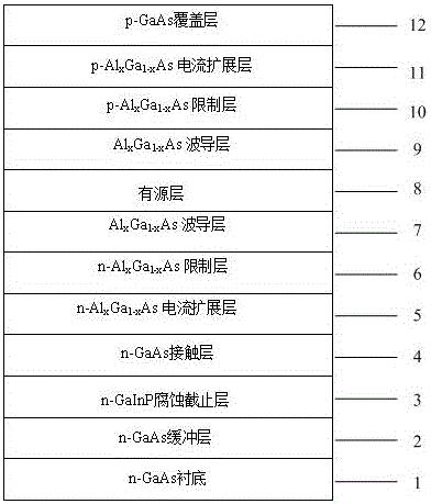
[0020] Such as figure 1 As shown, each layer is epitaxially grown on the n-GaAs substrate from bottom to top by metal organic chemical vapor deposition (MOCVD) method.

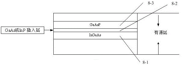
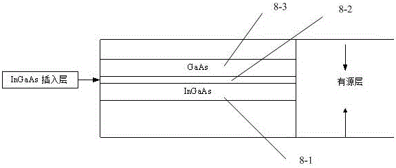
[0021] On n-GaAs substrate 1, epitaxially grow n-GaAs buffer layer 2 from bottom to top, n-GaInP etch stop layer 3, n-GaAs contact layer 4, n-Al x Ga 1-x As current spreading layer 5, n-Al x Ga 1-x As lower confinement layer 6, Al x Ga 1-x As lower waveguide layer 7, active layer 8, Al x Ga 1-x As on the waveguide layer 9, p-Al x Ga 1-x Confinement layer 10 on As, p-Al x Ga 1-x As current spreading layer 11, p-GaAs cladding layer 12.

[0022] Wherein: n-GaAs substrate 1 is an N-type GaAs material of (100) plane.

[0023] The n-GaInP etch stop layer 3 has a thickness of 200nm and adopts Si 2 h 6 as a source of doping.

[0024] n-Al x Ga 1-x The thickness of the As current spreading layer 5 is between 1000nm and 10000nm, and 02 h 6 as a source of doping.

[002...


PUM


Abstract

The invention discloses an epitaxial wafer for a flip infrared light-emitting diode, and belongs to the technical field of epitaxy of light emitting diodes. Layers are epitaxially formed on the same side of a substrate in sequence; an active layer comprises InGaAs quantum well layers and GaAsP barrier layers which alternate periodically; the period number is 2 to 6; the active layer adopts an InGaAs/GaAsP strain compensation quantum well structure; the strain compensation quantum well can restrain carriers to flow in place transversely to form non-radiative recombination by mistake, so that the quantum efficiency is improved.

Description

technical field [0001] The invention belongs to the technical field of epitaxial extension of light-emitting diodes, in particular to a method for preparing epitaxial wafers for flip-chip infrared light-emitting diodes. Background technique [0002] Infrared light-emitting diodes are diodes that can emit infrared rays. They are used in security monitoring, wearable devices, infrared communications, infrared remote control devices, light sources for sensors, and night lighting, especially in the field of gas detection. Using the InGaAs / GaAsP strain compensation multi-quantum well structure and the InGaAs / GaAs strained quantum well structure as the active layer, a light emitting diode with a light emitting wavelength above 850nm can be prepared. [0003] During the growth of strain-compensated quantum well materials, InGaAs and GaAsP will diffuse each other at the interface, and it is difficult to obtain quantum wells and quantum barrier layers with better interface quality, s...

Claims


Application Information

Patent Timeline
Patent Type & Authority Applications(China)
IPC IPC(8): H01L33/06H01L33/12H01L33/30
CPCH01L33/06H01L33/12H01L33/30
Inventor 田海军林鸿亮赵宇石峰杨凯张双翔
Owner YANGZHOU CHANGELIGHT
Why Eureka
Try Eureka