End-coupling nano optical waveguide type dual-optical-path chip-scale atomic clock

A chip-level atomic clock and end-face coupling technology, which is applied in the field of optics and micro-nano systems, can solve the problems of reducing the short-term frequency stability of chip-level atomic clocks, large amplitude noise, and large fluctuation noise of optical frequency, so as to improve the short-term stability, The effect of improving mid- and long-term stability and reducing optical power fluctuation and frequency fluctuation noise

Inactive Publication Date: 2017-01-11
ZHONGBEI UNIV
View PDF12 Cites 4 Cited by
  • Summary
  • Abstract
  • Description
  • Claims
  • Application Information

AI Technical Summary

Problems solved by technology

Although the influence of optical frequency noise fluctuation can be greatly reduced by locking the VCSEL laser to the transition line of the atom, the optical frequency fluctuation noise is still very large
Second, in some VCSELs, mode competition noise between different polarization modes can cause large amplitude noise on the detector
All this noise degrades the short-term frequency stability of chip-scale atomic clocks, leading to the current use of 1mm 3 The best second-order stability achieved by the chip atomic clock in the gas chamber is at 10 -11 magnitude

Method used


Image

  • End-coupling nano optical waveguide type dual-optical-path chip-scale atomic clock
  • End-coupling nano optical waveguide type dual-optical-path chip-scale atomic clock
  • End-coupling nano optical waveguide type dual-optical-path chip-scale atomic clock

Examples


Embodiment 1

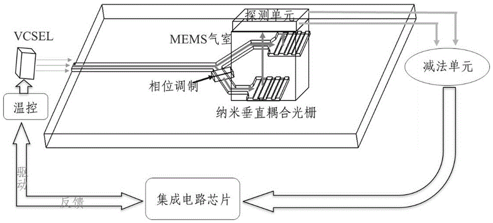
[0022] A vertically coupled nano-optical waveguide dual-optical chip-scale atomic clock (single gas chamber), such as image 3 As shown, it includes a VCSEL laser 13, the light beam emitted by the VCSEL laser 13 is coupled into the Y-waveguide beam splitter 16 through the end-face coupling input port 10, and the end-face coupling input port realizes the coupling input of the VCSEL collimated and isolated laser light source (the coupling efficiency is excellent 80%), through the coupling alignment technology and the nano-Y-type waveguide for precise docking; one of the beams of light passes through the phase modulation unit 15 (modulation electrode) to generate coherent light with a constant phase difference and then output, and the other beam of light is adjusted by the ohmic electrode The output is compensated in accordance with the modulation optical path. For example, one path of guided wave beam can be modulated at 3.4GHz to produce a sideband with a frequency difference of...

Embodiment 2

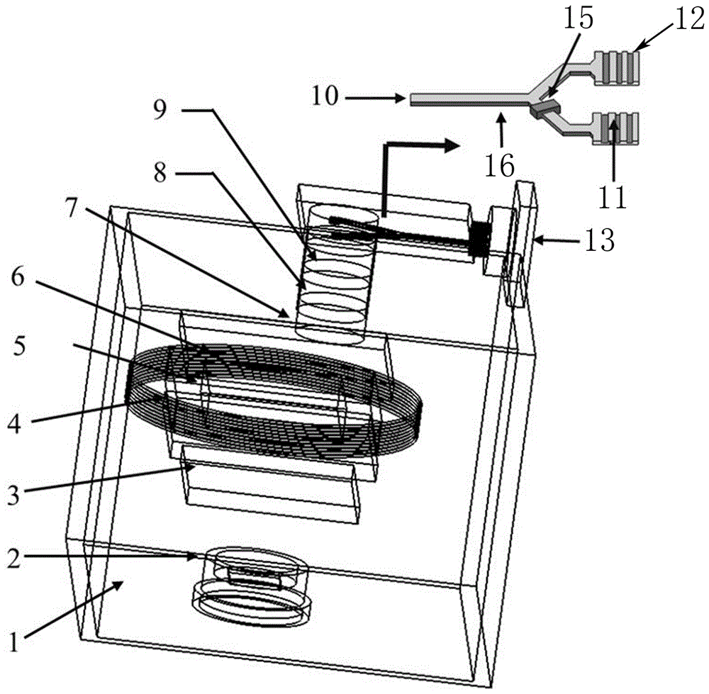
[0026]A vertically coupled nano-optical waveguide dual optical path chip-scale atomic clock (dual gas chamber), which differs from Embodiment 1 in that it adopts double gas chambers, adopts on-site preparation of rubidium atoms, and puts reaction medicine 18 in reaction gas chamber 17 to prepare The rubidium atom gas enters into the photoaction gas chamber 14. The rest of the principles are the same as in Embodiment 1. The two beams of light emitted from the micro-air chamber reach the two-phase detection chips at the same time, that is, the detection unit 2 converts it into an electrical signal and then inputs it into the subtractor. Subtracting the signals is a clock that eliminates common-mode noise The signal is input to the integrated circuit chip, and the integrated circuit chip completes the regulation of the laser and the phase modulation unit. The subtractor and the integrated circuit chip are integrated in the circuit module 19, and output the control signal through t...


PUM


Abstract

The invention discloses an end-coupling nano optical waveguide type dual-optical-path chip-scale atomic clock comprising a laser device. An emergent light beam of the laser device enters a Y-waveguide beam splitter through coupling of the end-coupling input end, wherein one light beam is outputted after passing through a phase modulation unit while the other light beam is outputted after adjust compensation, and the two light beams are outputted after passing through a vertical coupling grating II and a vertical coupling grating III respectively and sequentially pass through a polaroid, attenuation slices, a wave plate, collimation and focusing prior to entering an air chamber. After being emergent, the two light beams are converted into electrical signals through a detection unit, the electrical signals are inputted into an integrated circuit chip through a subtracter, and the integrated circuit chip is used for regulating and controlling the laser device and the phase modulation unit. The end-coupling nano optical waveguide type dual-optical-path chip-scale atomic clock has the advantages that the effect of optical power fluctuation and frequency fluctuation noise can be greatly weakened and the signal-to-noise ratio of the CPT atomic clock can be effectively improved through dual-optical-path common-mode rejection, so that short-term stability of the chip-scale atomic clock can be greatly enhanced.

Description

technical field [0001] The invention belongs to the field of optics and the field of micro-nano systems, in particular to an end-face coupled nano-optical waveguide dual optical path chip-level atomic clock based on the CPT effect. Background technique [0002] As a new type of atomic frequency standard, the chip atomic clock based on the CPT principle can ensure the relative position measurement and precise time synchronization between satellites in the mobile communication constellation. At present, major foreign research institutes and companies have invested energy in developing new structures and new processes of CSAC in order to further reduce the volume and reduce power consumption. It can be seen from foreign research results that the current development performance parameters of chip atomic clocks basically meet some application requirements, and commercial chip atomic clock products have been developed, and great progress has been made. It is difficult to further ...

Claims


Application Information

Patent Timeline
Patent Type & Authority Applications(China)
IPC IPC(8): G04F5/14
CPCG04F5/14
Inventor 闫树斌张志东崔建功汤跃张文栋薛晨阳
Owner ZHONGBEI UNIV
Why Eureka
Try Eureka