

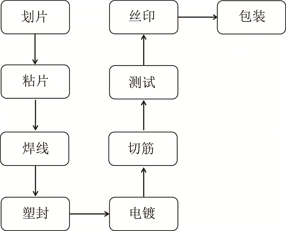
Diode packaging process
A preparation process and diode technology, which is applied in semiconductor/solid-state device manufacturing, electrical components, circuits, etc., can solve the problems of zero utilization of empty pins, inconvenient production and application of integrated circuit boards, etc., and achieve the advantages of reducing quantity and improving quality , good quality effect
- Summary
- Abstract
- Description
- Claims
- Application Information
AI Technical Summary
Problems solved by technology
Method used
Image

Examples
Embodiment 1
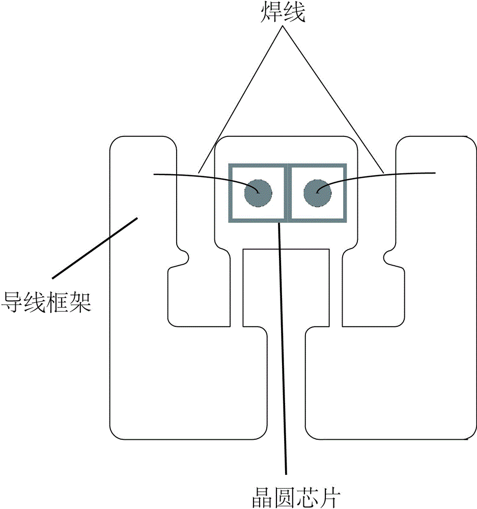
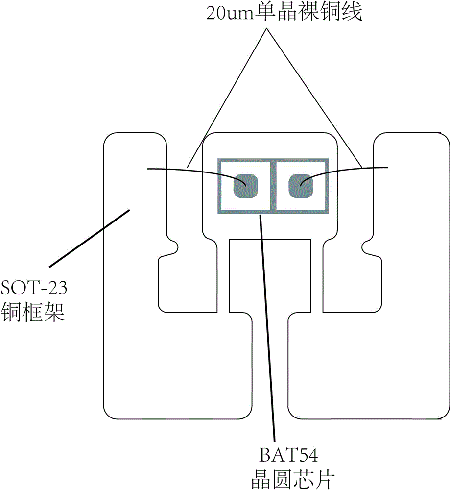
[0033] Embodiment 1. A kind of Schottky diode, product model is BAT54, adopts SOT-23 package, and wafer is a 4-inch chip, and the concrete implementation production process is as follows:
[0034] (1) Scribing: Take out the coated wafer from the nitrogen protection cabinet for standby, first perform wafer grinding, remove the wafer surface film, place the wafer on the workbench of the high-speed dicing machine, and calibrate the high-speed dicing According to the camera angle of the machine, the scribing lane size required for a 4-inch wafer is 50um and the chip size is 350um*350um, and the width of the cutting lane is set. The width of the axis dicing is 50um for the scribing lane of a single chip. After the width of the dicing lane is set, the wafer is cut. The workbench carrying the wafer moves in a 90° straight line along the tangential direction of the contact point between the blade and the wafer. Turn on the water washing function and use deionized water to rinse the si...
Embodiment 2
[0043] Embodiment 2. A kind of switching diode, product model is BAV99, adopts SOT-23 package, and wafer is a 4-inch chip, and the concrete implementation production process is as follows:
[0044] (1) Scribing: Take out the coated wafer from the nitrogen protection cabinet for standby, first perform wafer grinding, remove the wafer surface film, place the wafer on the workbench of the high-speed dicing machine, and calibrate the high-speed dicing According to the camera angle of the machine, the dicing lane size required for a 4-inch wafer is 40um and the chip size is 280um*280um, and the width of the cutting lane is set. The width of the axis dicing is 40um, and the scribing lane size of a single chip is 40um. After the width of the dicing lane is set, the wafer is cut. The workbench carrying the wafer moves in a 90° straight line along the tangential direction of the contact point between the blade and the wafer. Turn on the water washing function and use deionized water to...
Embodiment 3
[0053] Embodiment 3. A kind of zener diode, product model is AZ23C2V7, adopts SOT-23 package, and wafer is a 4-inch chip, and the concrete implementation production process is as follows:
[0054] (1) Scribing: Take out the coated wafer from the nitrogen protection cabinet for standby, first perform wafer grinding, remove the wafer surface film, place the wafer on the workbench of the high-speed dicing machine, and calibrate the high-speed dicing According to the camera angle of the machine, the scribing lane size required for a 4-inch wafer is 50um and the chip size is 350um*350um, and the width of the cutting lane is set. The width of the axis dicing is 50um for the scribing lane of a single chip. After the width of the dicing lane is set, the wafer is cut. The workbench carrying the wafer moves in a 90° straight line along the tangential direction of the contact point between the blade and the wafer. Turn on the water washing function and use deionized water to rinse the si...
PUM
 Abstract
Description
Claims
Application Information