Planar lateral collection structure indium gallium arsenic infrared detector chip

An infrared detector, indium gallium arsenic technology, applied in the direction of semiconductor devices, electrical components, circuits, etc., can solve the problems of detector dark current and blind element rate reduction, increase the defect density of epitaxial layer, and diffuse thermal damage on the surface of the device. Achieve the effect of reducing dark current and blind element rate, reducing diffusion heat damage, and uniformly reducing photosensitive element response

Inactive Publication Date: 2017-01-11
NANTONG UNIVERSITY
View PDF3 Cites 3 Cited by
  • Summary
  • Abstract
  • Description
  • Claims
  • Application Information

AI Technical Summary

Problems solved by technology

However, this preparation process makes the surface of the device prone to thermal damage due to diffusion during the high-temperature diffusion process. In addition, the out-diffusion of Zn and P elements in the subsequent heat treatment process increases the defect density in the epitaxial layer, resulting in the deterioration of the PN junction. Poor, which largely limits the further reduction of detector dark current and blind cell rate

Method used


Image

  • Planar lateral collection structure indium gallium arsenic infrared detector chip
  • Planar lateral collection structure indium gallium arsenic infrared detector chip
  • Planar lateral collection structure indium gallium arsenic infrared detector chip

Examples


Embodiment Construction

[0018] The technical solution of the present invention will be described in detail below in conjunction with the accompanying drawings.

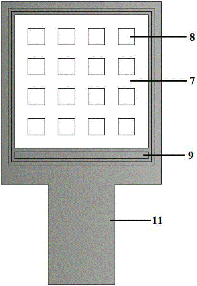
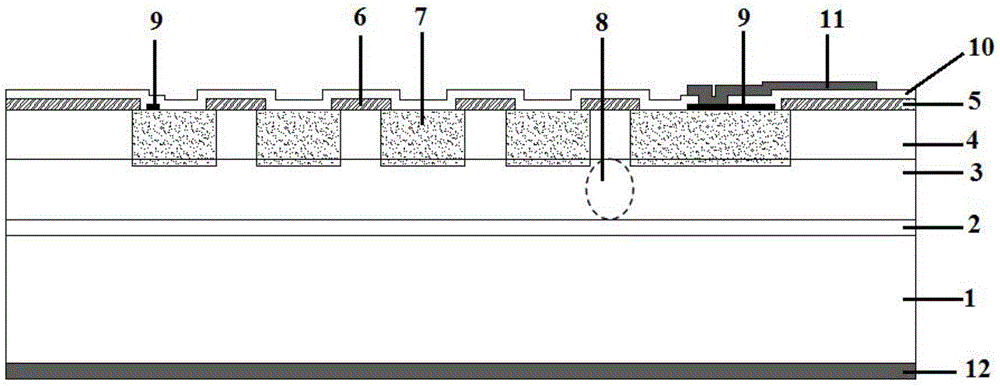
[0019] as attached figure 2 As shown, the epitaxial wafers used in this embodiment are metal-organic chemical vapor deposition (MOCVD) technology with a thickness of 300 μm and a carrier concentration of >3×10 18 cm -3 An N-type InP layer 2 with a thickness of 0.5 μm is sequentially grown on the N-type InP substrate 1, and the carrier concentration is >2×10 18 cm -3 ; InGaAs intrinsic absorption layer 3 with a thickness of 2.5 μm and a carrier concentration of 5×10 16 cm -3 ; N-type InP capping layer 4 with a thickness of 1 μm and a carrier concentration of 5×10 16 cm -3 . The carrier lateral collection diffusion barrier region 6 in this embodiment is a 4×4 array structure, and the size of each barrier region is 10×10 μm 2 .

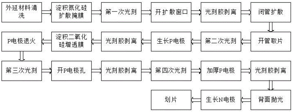
[0020] The specific preparation process steps of the chip of this embodiment are as follows ( image 3 sho...


PUM


Abstract

The invention discloses a planar lateral collection structure indium gallium arsenic infrared detector chip which comprises an N-type InP substrate, an N-type InP layer, an indium gallium arsenic intrinsic absorption layer, an N-type InP cap layer, a silicon nitride diffusion covering film layer, at least two rectangular carrier lateral collection diffusion barrier regions, a PN nodal region formed by diffusion and a carrier lateral collection region. A single Au layer grows on the periphery of a photosensitive unit to form a P electrode, silicon dioxide is deposited on the surface of the chip to form a silicon dioxide transmission enhanced layer, a P electrode hole is opened by a wet etching process, Cr and Au sequentially grow to form a thickened electrode, the edge length of each carrier lateral collection diffusion barrier region is 5-10 micrometers, the carrier lateral collection diffusion barrier regions are arranged in an aligned or area arrayed manner and are the same in center distance, and the P electrode and the thickened electrode are annular covering electrodes and are the same in inside dimension. Heat diffusion regions are decreased, so that heat diffusion loss is effectively decreased, and the dark current and the blind-pixel rate of a device are reduced while response uniformity of the photosensitive unit is kept.

Description

technical field [0001] The invention relates to an infrared detector chip, in particular to an indium gallium arsenide infrared detector chip with a planar lateral collection structure. Background technique [0002] InGaAs short-wave infrared detectors can work at room temperature and have broad application prospects in civil, military and aerospace fields. At present, PIN InGaAs detectors are mainly divided into two types: planar type and mesa type. Due to the difficulty of passivation on the side of the mesa device, the reliability of the device is reduced and the dark current is large, which limits the improvement of the detection rate of the device to a large extent. Planar detectors are the mainstream structure of InGaAs detectors. The PN junction region of the device is mainly prepared by Zn high-temperature diffusion in n-InP / i-InGaAs / n-InP epitaxial materials, which has the advantages of easy passivation, dark current Low cost, high reliability and other advantages...

Claims


Application Information

Patent Timeline
Patent Type & Authority Applications(China)
IPC IPC(8): H01L31/101H01L31/0352H01L31/0304
CPCH01L31/101H01L31/03046H01L31/0352
Inventor 邓洪海郭兴龙杨清华杨波王强马青兰邵海宝王志亮尹海宏黄静李毅李雪龚海梅
Owner NANTONG UNIVERSITY
Why Eureka
Try Eureka