

Curing adhesive used for preparation of microsection sample of printed circuit and preparation method thereof
A technology for metallographic slicing and printed circuits, applied in the direction of adhesives, non-polymer organic compound adhesives, etc., can solve the problems of complicated manufacturing process, high cost, poor transparency of cured products, etc., and achieve high bonding strength , low cost, good transparency
- Summary
- Abstract
- Description
- Claims
- Application Information
AI Technical Summary
Problems solved by technology
Method used
Image

Examples
Embodiment 1
[0028] A component
[0029] Weigh 10 g of polymethyl methacrylate, add 0.1 g of benzoyl peroxide and 0.05 g of sodium lauryl sulfate to it, grind and mix evenly with a mortar;
[0030] B component
[0031] 4g of methyl methacrylate with a purity of 99.0% and 2g of acetone with a purity of 99.5% were weighed, and 0.01g of N,N-dimethyl-p-toluidine was added dropwise thereto, and stirred and mixed evenly.
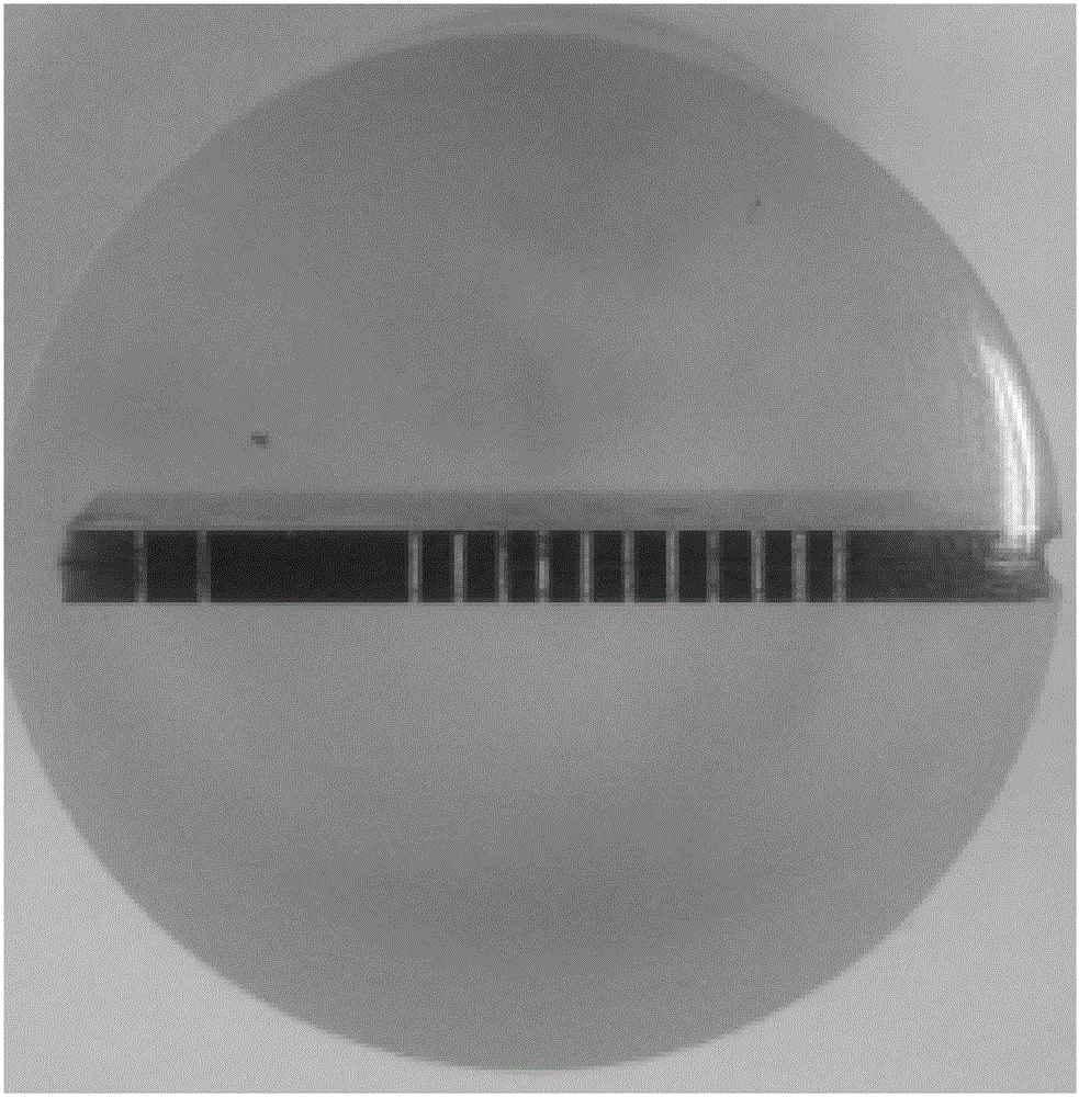
[0032] Put the above-prepared components A and B in a mosaic mold with an inner diameter of 25 mm and a height of 22 mm at a mass ratio of 2:1, and cure at room temperature for 30 minutes. like figure 1 As shown, it is a transparent effect diagram of the mosaic slice after the cured glue is mixed and cured in this embodiment.
Embodiment 2
[0034] A component
[0035] Weigh 20 g of polymethyl methacrylate; add 0.15 g of benzoyl peroxide and 0.05 g of sodium dodecylbenzene sulfonate to it, and mix well.
[0036] B component
[0037] 8 g of methyl methacrylate with a purity of 99.0% and 4 g of ethyl acetate with a purity of 99.5% were weighed, and 0.03 g of N,N-dimethylaniline was added thereto, and stirred and mixed uniformly.
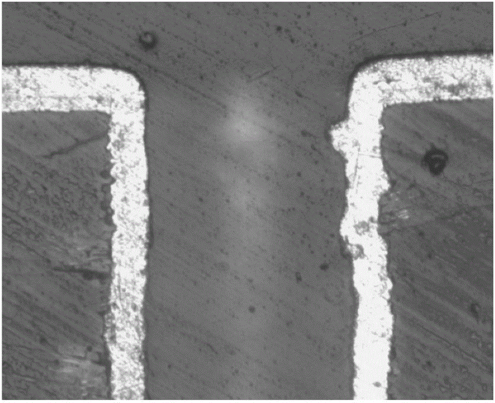
[0038] Put the above-prepared components A and B in a mosaic mold with an inner diameter of 25 mm and a height of 22 mm at a mass ratio of 2:1, and cure at room temperature for 30 minutes. like figure 2 As shown, it is the effect diagram of the cured glue of this embodiment used for metallographic section observation of the metallographic structure.
PUM
 Abstract
Description
Claims
Application Information