Multilayer SOI material and preparation method thereof

A H2SO4, underlying technology, applied in semiconductor/solid-state device manufacturing, electrical components, circuits, etc., can solve problems such as poor quality of silicon wafers, stacking restrictions on the number of layers, edge bonding of silicon wafers, etc., and achieve the effect of small edge loss

Active Publication Date: 2017-02-15
SHENYANG SILICON TECH
View PDF7 Cites 14 Cited by
  • Summary
  • Abstract
  • Description
  • Claims
  • Application Information

AI Technical Summary

Problems solved by technology

The traditional SOI manufacturing technology needs to go through many times of high temperature. The more times of high temperature, the worse the quality of each layer of silicon wafer will be.
As the number of layers increases, the stress inside SOI will also increase, which greatly limits the stacking of l...

Method used


Image

  • Multilayer SOI material and preparation method thereof
  • Multilayer SOI material and preparation method thereof
  • Multilayer SOI material and preparation method thereof

Examples


Embodiment 1

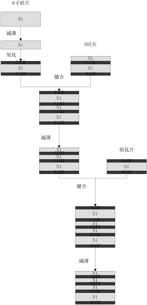
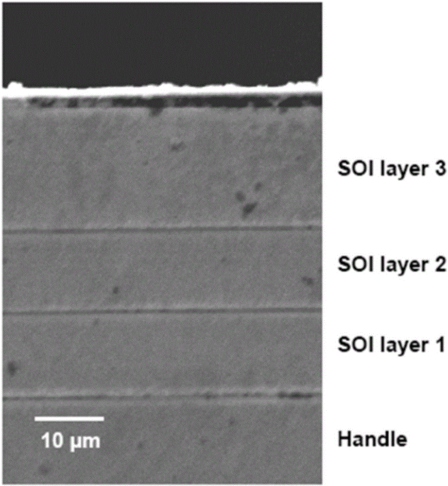
[0034] This embodiment is the preparation of 6-inch 3-layer SOI material, and the process is as follows ( figure 1 ):

[0035] (1) Take a 6-inch, N-type, resistivity 4-7ohm.cm, crystal orientation silicon wafer, and thin it to 400μm. Then oxidize, the oxide layer is 0.5μm.

[0036] (2) Choose a piece of 6-inch SOI: the top silicon thickness is 10μm, N type, resistivity 8-12ohm.cm, crystal orientation ; the middle oxide layer silicon dioxide is 0.5μm; the substrate silicon thickness is 675μm, N Type, resistivity 8-12ohm.cm, crystal orientation .

[0037] (3) Carry out CMP stress relief treatment (treatment time 180 seconds, polishing pressure 20KPa) to the oxide layer on the silicon chip in step (1), then carry out 3min surface treatment with DHF, carry out plasma activation again (using N 2 , gas pressure 0.3mbar, activation time 5s, RF power 75W). Use concentrated H on the SOI sheet of step (2) 2 SO 4 Treat at 120°C for 3 minutes without plasma activation; then bond th...


PUM

PropertyMeasurementUnit
Layer thicknessaaaaaaaaaa
Thicknessaaaaaaaaaa
Thicknessaaaaaaaaaa

Abstract

The invention discloses a multilayer SOI material and a preparation method thereof, and belongs to the technical field of semiconductor material preparation. The material is a multilayer SOI stacked structure, the top surface and the bottom surface of the stacked structure are silicon chips, and the middle portion is formed by alternative arrangement of silicon chips and BOX layers. In a preparation process, the stress of an oxidation sheet is removed through a CMP method, and bonding of the multilayer SOI can be stacked on the oxidation sheet. Surface treatment of the silicon chip with the surface of the oxidation sheet is performed for 1-5 minutes by employing HF, and plasma activation treatment is also performed; and surface treatment of the silicon chip with the surface of the silicon chip is performed for 1-5 minutes by employing concentrated H2SO4. After the treatment, normal-temperature bonding is then performed, low-temperature annealing can be performed at the temperature of lower than 500 DEG C, extremely good bonding quality is obtained, and the edge loss is less than 0.5 mm in the subsequent thinning process. The whole bonding process is accomplished at a low temperature, and the multi-layer SOI device layer is prevented from high temperature so that defects can be avoided.

Description

technical field [0001] The invention relates to the technical field of semiconductor material preparation, in particular to a multilayer SOI material and a preparation method thereof. Background technique [0002] SOI (Silicon On Insulator, silicon on insulating layer) technology introduces a buried oxide layer (BOX layer) between the top silicon and the back substrate. Due to its complicated manufacturing process and high cost, its technology has been adopted by foreign countries. Monopolized by a few countries, its application has been high in high-end products such as military, space and cutting-edge electrical appliances. In recent years, with the advancement of SOI manufacturing technology and the reduction of cost, silicon-on-insulator SOI has gradually moved towards the stage of commercial application and opened up the civilian market. It has become a necessary base material for new products in the IT industry. Especially in the 21st century, silicon-on-insulator SOI...

Claims


Application Information

Patent Timeline
IPC IPC(8): H01L21/02
CPCH01L21/02532H01L21/02664
Inventor 陈学斌柳清超毛俭
Owner SHENYANG SILICON TECH
Why Eureka
Try Eureka