Semiconductor structure and method for forming same

A semiconductor and graphic technology, applied in semiconductor devices, semiconductor/solid-state device manufacturing, semiconductor/solid-state device components, etc., can solve the problems of semiconductor structure and performance to be improved, and achieve the effect of simple process

Active Publication Date: 2017-02-15
SEMICON MFG INT (SHANGHAI) CORP +1
View PDF5 Cites 0 Cited by
  • Summary
  • Abstract
  • Description
  • Claims
  • Application Information

AI Technical Summary

Problems solved by technology

[0004] Although the use of copper metal as the material of the interconnect structure in the semiconductor structure can improve the performance of the semiconductor structure to a certain extent, the performance of the semiconductor structure still needs to be improved

Method used


Image

  • Semiconductor structure and method for forming same
  • Semiconductor structure and method for forming same
  • Semiconductor structure and method for forming same

Examples


Embodiment Construction

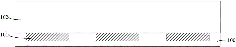
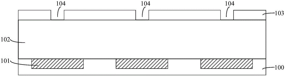
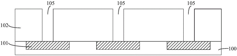
[0030] It can be seen from the background art that the performance of the semiconductor structure formed in the prior art needs to be further improved.

[0031] It has been found through research that although copper metal is more suitable than aluminum metal as a material for the interconnection structure in the conductor structure, the resistance of the semiconductor structure is still relatively high due to the high resistivity of copper metal.

[0032] Further studies have found that graphene is a two-dimensional crystal composed of carbon atoms on a single-layer honeycomb crystal lattice. Graphene not only has excellent mechanical properties and thermal stability, but also has excellent electrical properties, such as Submicron-scale ballistic transport properties, high carrier mobility, tunable band gap, quantum Hall effect at room temperature, etc., and graphene also has the advantage of low resistivity.

[0033] If the combination of graphene and copper can be used as t...


PUM

PropertyMeasurementUnit
thicknessaaaaaaaaaa
relative permittivityaaaaaaaaaa

Abstract

A semiconductor structure and a method for forming the same are provided. The method for forming the semiconductor structure comprises steps of: providing a substrate and a first dielectric layer on the surface of the substrate; forming an opening penetrating through the first dielectric layer; forming a first metal layer fully filling the opening and a second metal layer on the top surface of the first metal layer; forming a first graphene layer on the top surface and the sidewall surface of the second metal layer; forming a second dielectric layer on the top surface of the first dielectric layer, the top surface and the sidewall surface of the first graphene layer; grinding to remove the first graphene layer and the second dielectric layer higher than the top surface of the second metal layer until the top surface of the second metal layer is exposed; and forming a second graphene layer on the top surface of the exposed second metal layer. The method reduces the resistance of the semiconductor structure and improves the electrical performance of the semiconductor structure.

Description

technical field [0001] The invention relates to the technical field of semiconductor manufacturing, in particular to a semiconductor structure and a forming method thereof. Background technique [0002] With the continuous advancement of VLSI process technology, the feature size of semiconductor devices has been continuously reduced, and the performance of semiconductor devices has become stronger and stronger. The integration level of integrated circuit chips has reached hundreds of millions or even billions of devices. The above multilayer interconnection techniques are widely used. [0003] The traditional interconnection structure is made of aluminum metal, but as the size of semiconductors continues to shrink, smaller and smaller interconnection structures carry higher and higher currents, and the response time requirements of interconnection structures are getting higher and higher. The shorter, the traditional aluminum interconnect structure can no longer meet the re...

Claims


Application Information

Patent Timeline
Patent Type & Authority Applications(China)
IPC IPC(8): H01L21/768H01L23/532
CPCH01L23/53228H01L23/53276H01L21/76838H01L21/76877
Inventor 张海洋张城龙
Owner SEMICON MFG INT (SHANGHAI) CORP
Why Eureka
Try Eureka