OLED device and OLED display

A display and device technology, applied in the field of OLED devices and OLED displays, can solve the problems of unsuitability for displays, energy loss, complex preparation process, etc., and achieve the effects of increasing luminous intensity, increasing luminous intensity, and improving resolution

Inactive Publication Date: 2017-02-15
TCL CHINA STAR OPTOELECTRONICS TECH CO LTD
View PDF7 Cites 11 Cited by
  • Summary
  • Abstract
  • Description
  • Claims
  • Application Information

AI Technical Summary

Problems solved by technology

However, the preparation process of WOLED is complicated, and 2 / 3 of the light will be filtered out after passing through the color filter, resulting in energy loss. Moreover, the color purity of the three primary colors filtered by the color filter is poor, which is not suitable for production Color gamut (>100%) monitors
[0005] In addition, the luminous intensity of existing OLED devices is low, which is also not conducive to improving the display effect of OLED displays. figure 1 It is a schematic structural diagram of an existing common blue OLED device, which includes a transparent anode 100, a hole injection layer 200, a hole transport layer 300, an electron blocking layer 400, and a blue light emitting layer arranged sequentially from bottom to top. 500, the electron transport layer 600, and the cathode 700; the electron blocking layer 400, the blue light emitting layer 500, and the electron transport layer 600 constitute a blue light emitting unit, because the blue OLED device only has one blue light emitting unit, so the luminous intensity is higher Low, making the display effect of OLED display poor

Method used


Image

  • OLED device and OLED display
  • OLED device and OLED display
  • OLED device and OLED display

Examples


Embodiment Construction

[0044] In order to further illustrate the technical means adopted by the present invention and its effects, the following describes in detail in conjunction with preferred embodiments of the present invention and accompanying drawings.

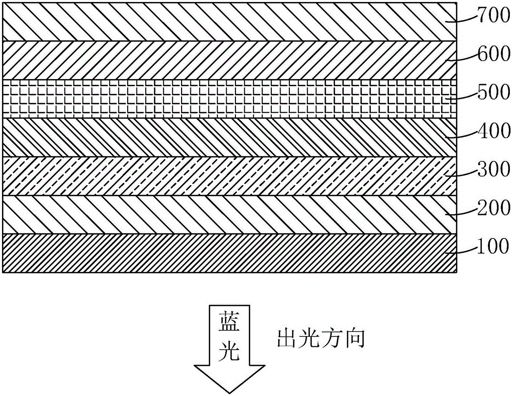
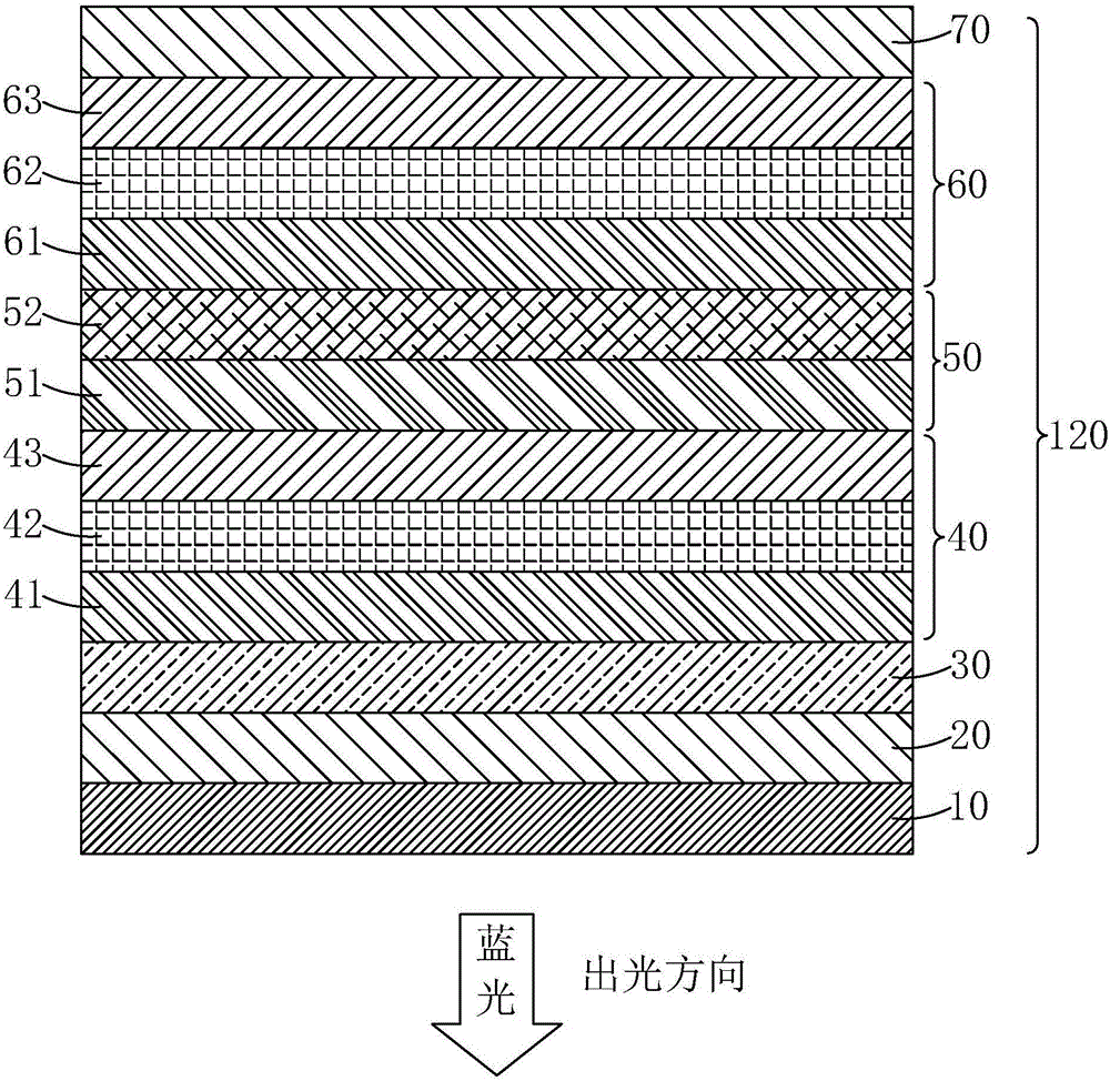
[0045] see figure 2 , the present invention firstly provides an OLED device 120, comprising an anode 10, a hole injection layer 20, a hole transport layer 30, a first light-emitting unit 40, a charge generation layer 50, and a second light-emitting unit 60 sequentially arranged from bottom to top , and cathode 70; the anode 10 is a translucent electrode;

[0046] The first light-emitting unit 40 includes a first electron blocking layer 41, a first light-emitting layer 42, and a first electron-transport layer 43 arranged in sequence from bottom to top; the second light-emitting unit 60 includes The second electron blocking layer 61, the second light emitting layer 62, and the second electron transport layer 63; the charge generation layer 50 ...


PUM


Abstract

The present invention provides an OLED device and an OLED display. The OLED device can increase the luminescent intensity of the OLED device by times through connecting two or more than two luminescent units in series; and a semitransparent anode is employed to introduce the microcavity effect to narrow the luminescence spectrum, make the light color purer and further improve the luminescent intensity. The OLED display includes the OLED device, the luminescent intensity is increased by times through connecting two or more than two luminescent units in series; the semitransparent anode is employed to introduce the microcavity effect to narrow the luminescence spectrum, make the light color purer and further improve the luminescent intensity so as to help to motivate a color conversion film to emit red and green light to obtain red, green and blue three-primary color lights with high color saturation and improve the color gamut of the OLED display; and because luminescent layers corresponding to red, green and blue pixels in the OLED display are blue luminescent layers, a precision metal mask version is avoided to use so as to facilitate improving the resolution ratio of the OLED display.

Description

technical field [0001] The invention relates to the field of display technology, in particular to an OLED device and an OLED display. Background technique [0002] OLED (Organic Light-Emitting Diode, organic light-emitting diode) display, also known as organic electroluminescence display, is a new flat panel display device, because of its simple preparation process, low cost, low power consumption, high luminous brightness, Wide range of working temperature, light and thin size, fast response speed, easy to realize color display and large-screen display, easy to realize matching with integrated circuit driver, easy to realize flexible display, etc., so it has broad application prospects. [0003] According to the driving method, OLED can be divided into two categories: passive matrix OLED (Passive Matrix OLED, PMOLED) and active matrix OLED (Active Matrix OLED, AMOLED), namely direct addressing and thin film transistor matrix addressing. Among them, AMOLED has pixels arrang...

Claims


Application Information

Patent Timeline
Patent Type & Authority Applications(China)
IPC IPC(8): H01L51/50H01L51/52
CPCH10K50/131H10K50/816H10K50/11H10K2101/10H10K50/852H10K59/00H10K50/80H10K50/00
Inventor 李先杰
Owner TCL CHINA STAR OPTOELECTRONICS TECH CO LTD
Why Eureka
Try Eureka