Method for optimizing growth of silicon carbide single crystals

A silicon carbide single crystal and crystal growth technology, applied in the direction of single crystal growth, single crystal growth, crystal growth, etc., can solve the problem of increasing crystal graphitization and forming other polytypes, dislocations and micro-pipes, and reducing crystal growth rate. , crystal growth rate limitation and other issues, to achieve the effect of promoting stable growth, inhibiting graphitization, and reducing defects

Inactive Publication Date: 2017-02-22
HEBEI SYNLIGHT CRYSTAL CO LTD
View PDF4 Cites 21 Cited by
  • Summary
  • Abstract
  • Description
  • Claims
  • Application Information

AI Technical Summary

Problems solved by technology

Graphitization of SiC powder will increase the possibility of crystal graphitization and the formation of other polytypes, dislocations and micropipes, making the crystal growth rate largely limited
Increasing the gas pressure in the growth chamber can inhibit the graphitization of SiC powder to a certain extent, but it will also reduce the growth rate of the crystal accordingly.

Method used


Image

  • Method for optimizing growth of silicon carbide single crystals

Examples


Embodiment 1

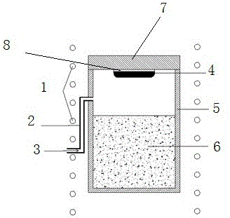
[0023] Example 1: A 4H-SiC single crystal was grown using an induction heating type PVT method single crystal furnace. The specific steps are as follows: (1) Drill a pore with a diameter of 6mm on the upper part of the side wall of the graphite crucible;

[0024] (2) Put the SiC raw material on the bottom of the graphite crucible, place the SiC seed crystal with a diameter of 4 inches on the graphite tray connected to the upper cover of the graphite crucible, the growth surface is the carbon surface, and the growth direction is the axial direction;

[0025] (3) Place the assembled crucible in the growth chamber of the single crystal furnace, one end of the graphite conduit is connected to the air hole on the side wall of the graphite crucible, and the other end is connected to the silane pipeline of the induction heating furnace;

[0026] (4) Vacuumize the graphite crucible before the silicon carbide crystal grows, so that the vacuum degree in the growth chamber reaches 1×10 -...

Embodiment 2

[0030] Example 2: A 6H-SiC single crystal was grown using an induction heating type PVT method single crystal furnace, and the specific steps were as follows: (1) Drilling a pore with a diameter of 6 mm on the upper part of the side wall of the graphite crucible;

[0031] (2) Put the SiC raw material on the bottom of the graphite crucible, place the SiC seed crystal with a diameter of 4 inches on the graphite tray connected to the upper cover of the graphite crucible, the growth surface is the carbon surface, and the growth direction is the axial direction;

[0032] (3) Place the assembled crucible in the growth chamber of the single crystal furnace, one end of the graphite conduit is connected to the air hole on the side wall of the graphite crucible, and the other end is connected to the silane pipeline of the induction heating furnace;

[0033] (4) Vacuumize the graphite crucible before the silicon carbide crystal grows, so that the vacuum degree in the growth chamber reache...


PUM

PropertyMeasurementUnit
diameteraaaaaaaaaa
diameteraaaaaaaaaa

Abstract

The invention belongs to the field of growth of silicon carbide single crystals, and particularly relates to a method for optimizing growth of the silicon carbide single crystals. The method includes the following steps: (1), drilling a gas hole in the upper portion of the side wall of a graphite crucible; (2), putting an SiC raw material at the bottom of the graphite crucible, and putting SiC seed crystals on a graphite tray connected with an upper cover of the graphite crucible; (3), connecting one end of a graphite guide pipe into the gas hole in the side wall of the graphite crucible, and connecting the other end of the graphite guide pipe to a silane pipe of an induction heating furnace; (4), performing vacuuming, keeping a vacuum state, injecting an exchange gas into a growth chamber, re-injecting the same flow of exchange gas for the same duration after 10-40 minutes, and cyclically repeating the process; (5), heating the growth chamber; (6), injecting silane gas into the growth chamber; (7), after growth of silicon carbide crystals, gradually decreasing the temperature of the growth chamber to room temperature. The method has the advantages that graphitization of the SiC raw material is inhibited, sublimate components are stably conveyed to a growth area, the growth process is optimized, and the defects in the crystals are reduced.

Description

technical field [0001] The invention belongs to the field of silicon carbide single crystal growth, and in particular relates to a method for optimizing silicon carbide single crystal growth. Background technique [0002] As a third-generation semiconductor material, silicon carbide single crystal has unique characteristics such as large band gap, strong radiation resistance, high breakdown electric field, small dielectric constant, high thermal conductivity, high electron saturation drift speed, and high chemical stability. , can be used to manufacture various high-frequency and high-power devices with high temperature resistance, and is used in occasions where silicon devices are incompetent. It is considered to be an ideal semiconductor material for manufacturing optoelectronic devices, high-frequency high-power devices, and power electronic devices. It is widely used in white light lighting, optical storage, screen display, aerospace, high temperature radiation environme...

Claims


Application Information

Patent Timeline
Patent Type & Authority Applications(China)
IPC IPC(8): C30B29/36C30B23/00
CPCC30B29/36C30B23/00
Inventor 牛晓龙杨昆高宇郑清超
Owner HEBEI SYNLIGHT CRYSTAL CO LTD
Why Eureka
Try Eureka