
Sealing ring of integrated circuit

An integrated circuit and sealing ring technology, applied in circuits, electrical components, electrical solid devices, etc., can solve the problems of unsatisfactory sealing ring, polysilicon density requirements, and capacitors occupying a large layout area, so as to increase capacitance and avoid uneven surface wrapping. network effect

Inactive Publication Date: 2017-02-22
SHANGHAI NATLINEAR ELECTRONICS CO LTD
View PDF3 Cites 4 Cited by
  • Summary
  • Abstract
  • Description
  • Claims
  • Application Information

AI Technical Summary

Problems solved by technology

[0008] In view of the above-mentioned shortcomings of the prior art, the purpose of the present invention is to provide an integrated circuit sealing ring, which is used to solve the problems in the prior art that the sealing ring does not meet the polysilicon density requirements and the capacitor occupies a large layout area.

Method used


Image

  • Sealing ring of integrated circuit
  • Sealing ring of integrated circuit
  • Sealing ring of integrated circuit

Examples


Embodiment 1

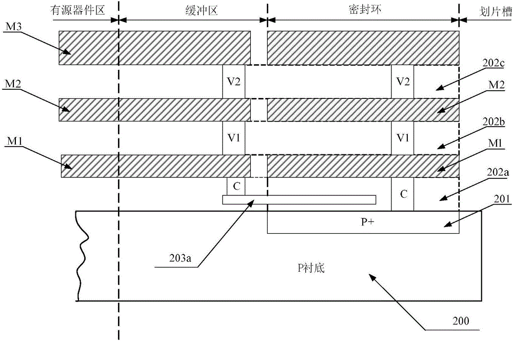
[0043] Such as image 3 As shown, the present invention provides an integrated circuit sealing ring, and the integrated circuit sealing ring at least includes:

[0044] A substrate layer 200 , a doped region 201 formed in the substrate layer 200 , a stacked structure of a dielectric layer and a metal layer formed on the doped region 201 , and a capacitor formed in the stacked structure.

[0045] Such as image 3 As shown, the substrate layer 200 is a P-type material substrate or an N-type material substrate. In this embodiment, the material of the substrate layer 200 is a P-type material, that is, trivalent elements such as boron are doped into the semiconductor ; while N-type materials are doped with phosphorus and other pentavalent elements in the semiconductor.

[0046] Such as image 3 As shown, the doped region 201 is formed on the surface layer of the substrate layer 200, and the doped region 201 is formed by performing heavy doping in the substrate layer 200, and the...

Embodiment 2

[0052] This embodiment provides an integrated circuit sealing ring. The structure of the integrated circuit sealing ring is basically the same as that of the sealing ring in Embodiment 1. The difference is that between any two adjacent metal layers, or the doping A second polysilicon and a third polysilicon are formed between the region and the underlying metal layer in the stacked structure, and the second polysilicon and the third polysilicon are vertically distributed.

[0053] Specifically, as Figure 5 As shown, in this embodiment, a second polysilicon 203b and a third polysilicon 203c are formed in the first dielectric layer 202a above the doped region 201, and the second polysilicon 203b and The third polysilicon 203c is distributed vertically, and the overlapping area of ​​the second polysilicon 203b and the third polysilicon 203c forms a PIP capacitor. The second polysilicon 203b and the third polysilicon 203c are respectively used as the first plate and the second p...

Embodiment 3

[0057] This embodiment provides an integrated circuit sealing ring. The structure of the integrated circuit sealing ring differs from the sealing rings in Embodiment 1 and Embodiment 2 in that a metal plate is formed between any two adjacent metal layers.

[0058] Specifically, as Figure 6 As shown, in this embodiment, a metal plate 204 is formed in the dielectric layer between the second metal layer M2 and the third metal layer M3, and the metal plate 204 intersects with the second metal layer M2 The overlapping area forms the MIM capacitor. The second metal layer M2 and the metal plate 204 serve as the first plate and the second plate of the capacitor respectively, and the capacity of the capacitor is related to the distance between the second metal layer M2 and the metal plate 204 . In this embodiment, the second metal layer M2 serves as the lower plate of the capacitor, and is electrically connected to the substrate layer 200 through the connection hole V1, the first met...


PUM


Abstract

The invention provides a sealing ring of an integrated circuit. The sealing ring comprises a substrate layer, a doping region, a laminated structure of dielectric layers and metal layers, and a capacitor, wherein the doping region is formed in the substrate layer; the laminated structure of dielectric layer and metal layers is formed on the doping region, and the metal layers and the doping region realize electrical connection through connecting holes; the capacitor is formed in the laminated structure, and a first pole plate and a second pole plate of the capacitor are connected with a substrate and an internal circuit through the metal layers in the laminated structure and metal layers in a buffer region respectively. According to the sealing ring of the integrated circuit provided by the invention, under the condition of not influencing the area of the integrated circuit or changing the function and performance of the sealing ring, the structure of an existing sealing ring of the integrated circuit is improved, so that the integrated circuit meets the density requirement of polycrystalline silicon and adds a filtering performance at the same time.

Description

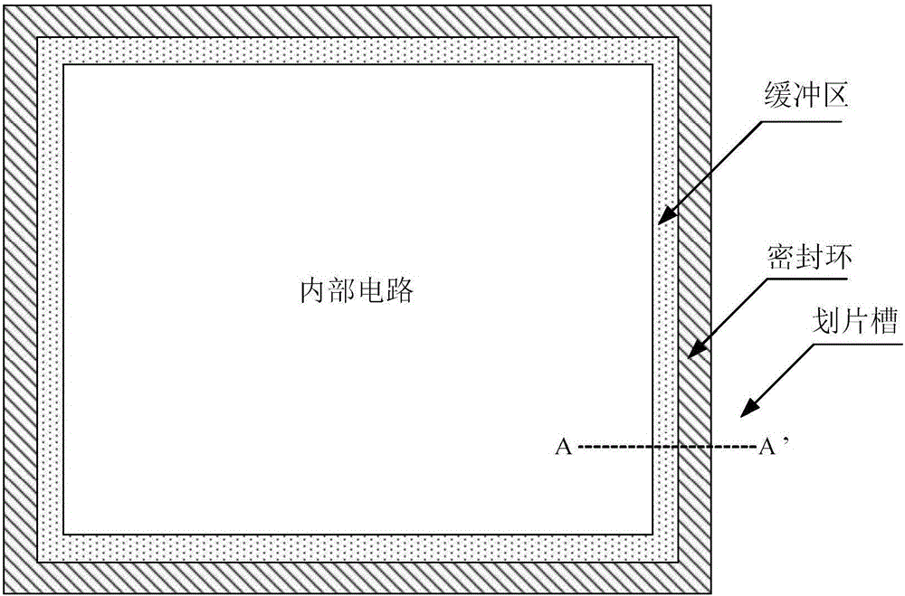
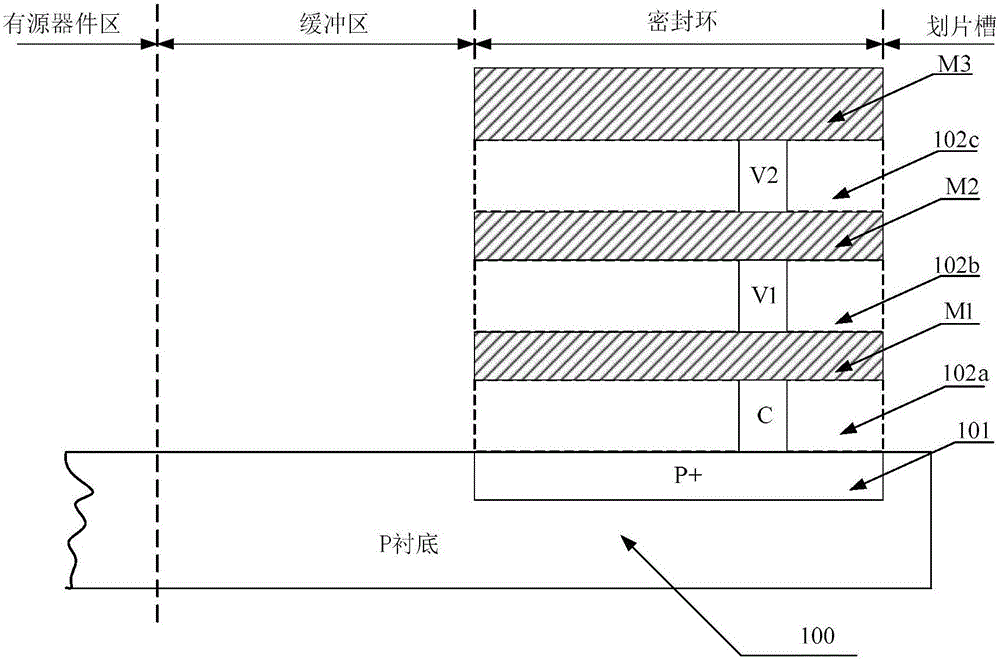
technical field [0001] The invention relates to the field of semiconductor manufacturing, in particular to an integrated circuit sealing ring. Background technique [0002] In a semiconductor manufacturing process, a semiconductor chip including a semiconductor active device and an interconnection structure disposed on the device can be formed on a semiconductor substrate through processes such as photolithography, etching, and deposition. Usually, multiple chips can be formed on a wafer, and finally these chips are cut off from the wafer, and integrated circuits are formed through a packaging process. [0003] During the process of dicing the chip, the stress generated by the dicing blade will cause damage to the edge of the chip, and even cause the chip to crack. In the prior art, in order to prevent the chip from being damaged during cutting, a sealing ring is provided around the active device area of ​​the internal circuit of the integrated circuit. The sealing ring can...

Claims


Application Information

Patent Timeline
IPC IPC(8): H01L23/58H01L23/64
CPCH01L23/585H01L23/642
Inventor 何云刘桂芝
Owner SHANGHAI NATLINEAR ELECTRONICS CO LTD
Learn More