Solar cell panel with graphene conducting layer

A solar panel and conductive layer technology, applied in the direction of circuits, photovoltaic power generation, electrical components, etc., can solve the problems of inconvenient cost, solar panels not integrated operation, etc., to achieve convenient control, convenient use and high efficiency, and reduce The effect of manual manipulation

Pending Publication Date: 2017-02-22
刘一锋
View PDF0 Cites 0 Cited by
  • Summary
  • Abstract
  • Description
  • Claims
  • Application Information

AI Technical Summary

Problems solved by technology

[0002] A solar cell is a device that responds to light and converts light energy into electricity. There are many materials that can produce photovoltaic effects, such as: single crystal silicon, polycrystalline silicon, amorphous silicon, gallium arsenide, indium selenium copper, etc. , and their power generation principles are basically the same. Now we take crystalline silicon as an example to describe the photoelectric power generation process. P-type crystalline silicon can be doped with phosphorus to obtain N-type silicon, forming a P-N junction. Absorption; the energy of the photon is transferred to the silicon atom, causing the electron to transition, becoming a free electron and gathering on both sides of the P-N junction to form a potential difference. When the external circuit is connected, under the action of the voltage, there will be a current flow A certain output power is generated through an external circuit. The essence of this process is: the process of converting photon energy into electrical energy, but the traditional solar panel does not realize integrated operation, which is not convenient enough and the cost is too high

Method used


Image

  • Solar cell panel with graphene conducting layer
  • Solar cell panel with graphene conducting layer
  • Solar cell panel with graphene conducting layer

Examples


Embodiment Construction

[0014] The following will clearly and completely describe the technical solutions in the embodiments of the present invention with reference to the accompanying drawings in the embodiments of the present invention. Obviously, the described embodiments are only some, not all, embodiments of the present invention. Based on the embodiments of the present invention, all other embodiments obtained by persons of ordinary skill in the art without making creative efforts belong to the protection scope of the present invention.

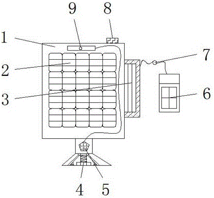
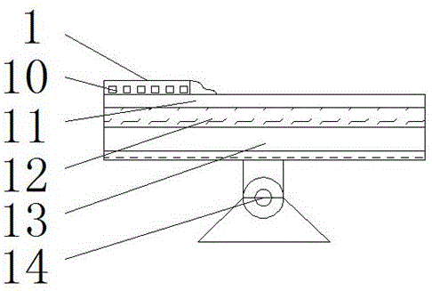
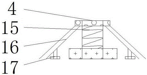
[0015] see Figure 1-3 , an embodiment provided by the present invention: a solar cell panel with a graphene conductive layer, including a working main body 1, a power device 3, a telescopic support 4 and a controller 6, and a working indicator light 8 is installed on the upper right of the working main body 1 , tempered glass 2 is installed on the outer side of the working body 1, an information collector 9 is installed above the toughened glass 2, a data pro...


PUM


Abstract

The invention discloses a solar cell panel with a graphene conducting layer. The solar cell panel comprises a main working body, a power device, a telescopic support, and a controller. A working indication lamp is installed right above the main working body; an information acquisition device is installed above a piece of armored glass; a data processor is installed at the lower side of the main working body; and the telescopic support is installed below the data processor. The telescopic support consists of a telescopic spring, an adjustable support, and an expansion bracket; the adjustable support is installed at one end of the telescopic spring; and the expansion bracket is installed at the lower end of the adjustable support. Besides, the power device is installed at one side of the main working body; and a PLC electric control unit is installed at one end of the power device that is connected with the controller by the PLC electric control unit. And the main working body includes an antireflection coating layer, an N pole silicon unit, a graphene conducting layer, a P pole silicon unit, and a rotatable turning device. According to the solar cell panel provided by the invention, on the basis of the internet-of-things technology, real-time controlling is carried out; an objective of rapid production is achieved to a great extent; and the integrated operation is realized.

Description

technical field [0001] The invention relates to the technical field of solar cell panel equipment, in particular to a solar cell panel with a graphene conductive layer. Background technique [0002] A solar cell is a device that responds to light and converts light energy into electricity. There are many materials that can produce photovoltaic effects, such as: single crystal silicon, polycrystalline silicon, amorphous silicon, gallium arsenide, indium selenium copper, etc. , their power generation principles are basically the same. Now we will take crystalline silicon as an example to describe the photoelectric power generation process. P-type crystalline silicon can be doped with phosphorus to obtain N-type silicon, forming a P-N junction. Absorption; the energy of the photon is transferred to the silicon atom, making the electron transition, becoming a free electron and gathering on both sides of the P-N junction to form a potential difference. When the external circuit i...

Claims


Application Information

Patent Timeline
Patent Type & Authority Applications(China)
IPC IPC(8): H02S20/30H02S50/00H01L31/0216
CPCH01L31/02168H02S20/30H02S50/00Y02E10/50
Inventor 刘一锋
Owner 刘一锋
Why Eureka
Try Eureka