Heat treatment method and heat treatment apparatus

A heat treatment method and technology of a heat treatment device, which are applied to semiconductor devices, electrical components, circuits, etc., can solve problems such as metal gate oxidation, silicon dioxide film thickness increase, etc., achieve short recovery pressure, increase production capacity, and heat treatment The effect of reaction homogenization

Active Publication Date: 2017-03-08
DAINIPPON SCREEN MTG CO LTD
View PDF6 Cites 5 Cited by
  • Summary
  • Abstract
  • Description
  • Claims
  • Application Information

AI Technical Summary

Problems solved by technology

[0009] In addition, when performing flash heat treatment on a semiconductor wafer with a metal gate deposited on a high dielectric constant film, there is also a problem that oxygen diffuses through the metal gate and the high dielectric constant film so that the base layer The film thickness of the silicon dioxide film increases, and the metal gate itself is oxidized

Method used


Image

  • Heat treatment method and heat treatment apparatus
  • Heat treatment method and heat treatment apparatus
  • Heat treatment method and heat treatment apparatus

Examples


no. 1 approach

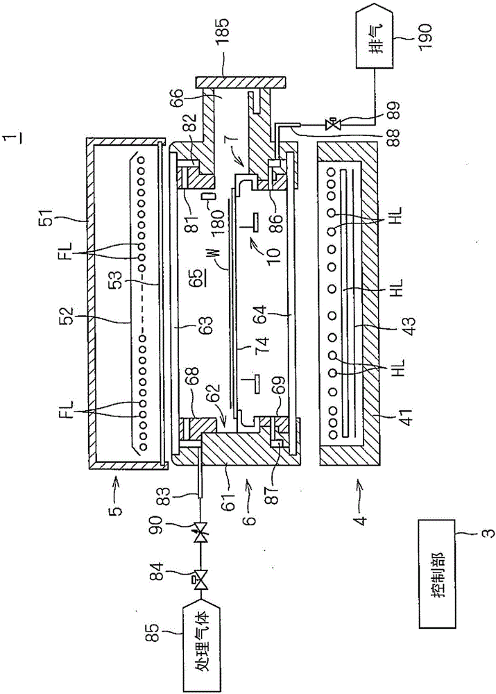
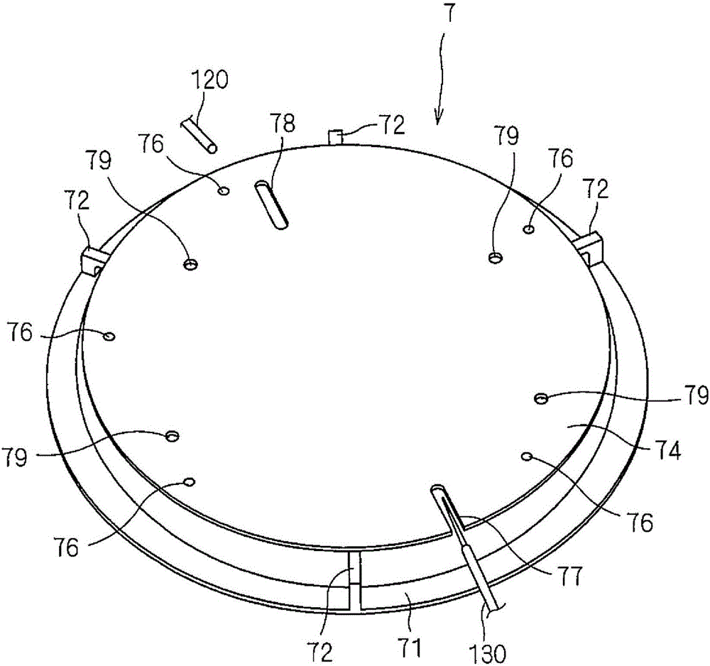
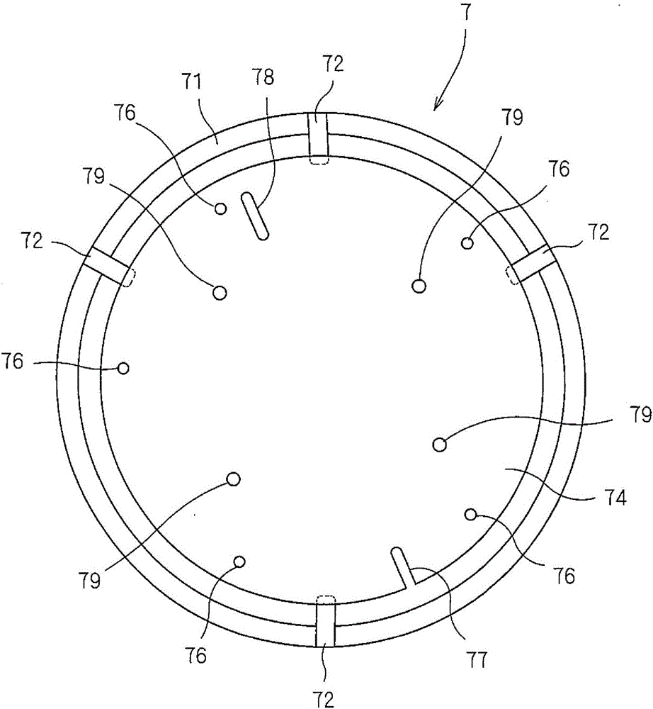
[0121] figure 1It is a longitudinal sectional view showing the structure of the heat treatment apparatus 1 of the present invention. The heat treatment apparatus 1 of this embodiment is a flash lamp annealing apparatus which heats the semiconductor wafer W by irradiating flash light to the disc-shaped semiconductor wafer W which is a board|substrate. The size of the semiconductor wafer W to be processed is not particularly limited, for example, or A high dielectric constant film is formed on the semiconductor wafer W before being carried into the heat treatment apparatus 1 , and post deposition annealing (PDA: Post Deposition Annealing) of the high dielectric constant film is performed by heat treatment of the heat treatment apparatus 1 . In addition, in figure 1 In each of the following figures, the size and quantity of each part are enlarged or simplified as necessary for ease of understanding.

[0122] The thermal processing apparatus 1 has a chamber 6 for accommodati...

no. 2 approach

[0186] Next, a second embodiment of the present invention will be described. The structure of the heat treatment apparatus 1 of the second embodiment is completely the same as that of the first embodiment. In addition, the processing procedure of the semiconductor wafer W in the thermal processing apparatus 1 of the second embodiment is also substantially the same as that of the first embodiment. The second embodiment differs from the first embodiment in that the pressure in the chamber 6 is restored after the pressure in the chamber 6 is decompressed once.

[0187] Figure 11 It is a figure which shows the pressure change in the chamber 6 in 2nd Embodiment. exist Figure 11 in, with Figure 10 Similarly, the horizontal axis represents the time, and the vertical axis represents the pressure in the chamber 6 . in addition, Figure 11 The pattern shown by the dotted line in is the pressure change pattern ( Figure 10 picture of).

[0188] As in the first embodiment, when...

no. 3 approach

[0201] Next, a third embodiment of the present invention will be described. The structure of the heat treatment apparatus 1 of the third embodiment is completely the same as that of the first embodiment. In addition, the processing procedure of the semiconductor wafer W in the thermal processing apparatus 1 of the third embodiment is also substantially the same as that of the first embodiment. The third embodiment differs from the first embodiment in that the pressure inside the chamber 6 changes.

[0202] Figure 12 It is a figure which shows the pressure change in the chamber 6 in 3rd Embodiment. exist Figure 12 in, with Figure 10 Similarly, the horizontal axis represents the time, and the vertical axis represents the pressure in the chamber 6 .

[0203] As in the first embodiment, when the semiconductor wafer W on which the high dielectric constant film 103 is formed is accommodated in the chamber 6 and the transfer opening 66 is closed, the pressure in the chamber 6...


PUM


Abstract

Over a front surface of a silicon semiconductor wafer is deposited a high dielectric constant film with a silicon oxide film, serving as an interface layer, provided between the semiconductor wafer and the high dielectric constant film. After a chamber houses the semiconductor wafer, a chamber's pressure is reduced to be lower than atmospheric pressure. Subsequently, a gaseous mixture of ammonia and nitrogen gas is supplied into the chamber to return the pressure to ordinary pressure, and the front surface is irradiated with a flash light, thereby performing post deposition annealing (PDA) on the high dielectric constant film. Since the pressure is reduced once to be lower than atmospheric pressure and then returned to ordinary pressure, a chamber's oxygen concentration is lowered remarkably during the PDA. This restricts an increase in thickness of the silicon oxide film underlying the high dielectric constant film by oxygen taken in during the PDA.

Description

technical field [0001] The present invention relates to a heat treatment method for heating a thin plate-shaped precision electronic substrate (hereinafter simply referred to as "substrate") such as a semiconductor wafer on which a high dielectric constant film or a metal gate is formed on a high dielectric constant film (hereinafter, simply referred to as a "substrate"). and heat treatment equipment. Background technique [0002] In the manufacturing process of semiconductor devices, flash lamp annealing (FLA), which heats a semiconductor wafer in an extremely short time, is attracting attention. Flash lamp annealing is a heat treatment technique that irradiates a flash of light on the surface of a semiconductor wafer using a xenon flash lamp (hereinafter referred to simply as a "flash lamp" means a xenon flash lamp) so that only the semiconductor wafer The surface of the wafer heats up. [0003] The radiation spectrum of the xenon flash lamp is distributed from the ultra...

Claims


Application Information

Patent Timeline
Patent Type & Authority Applications(China)
IPC IPC(8): H01L21/67H01L21/28H01L21/02
CPCH01L21/02345H01L21/28158H01L21/67115
Inventor 青山敬幸河原崎光古川雅志加藤慎一布施和彦谷村英昭
Owner DAINIPPON SCREEN MTG CO LTD
Why Eureka
Try Eureka