AMOLED pixel driving circuit and pixel driving method

A technology of pixel driving circuit and power supply, applied in instruments, static indicators, etc., can solve the problems of reference signal or initialization signal loss, affecting panel compensation effect, panel loss of compensation effect, etc., to improve panel yield, reduce loss, Loss reduction effect

Active Publication Date: 2017-03-15
TCL CHINA STAR OPTOELECTRONICS TECH CO LTD
View PDF4 Cites 11 Cited by
  • Summary
  • Abstract
  • Description
  • Claims
  • Application Information

AI Technical Summary

Problems solved by technology

[0016] Usually in the circuit layout design, the signal on the reference signal line or the initialization signal line is provided by the peripheral integrated circuit (integrated circuit, IC) or flexible circuit board (Flexible Printed Circuit, FPC), providing the input point of the reference signal or initialization signal It is usually located at the four corners of the panel, and usually enters the plane in the form of a simple horizontal or vertical connection. This connection may cause loss of the reference signal or initialization signal during the wire transmission process, that is, the received signal in the center of the panel The value of the reference signal or initialization signal received will be smaller than the corresponding signal received by the edge of the panel, and the greater the impedance of the wire, the greater the difference, which will affect the compensation effect of the panel; at the same time, this wiring method increases the wiring in the panel Quantity, it is easy to cause a short circuit between the wires, causing the entire panel to lose the compensation effect

Method used


Image

  • AMOLED pixel driving circuit and pixel driving method
  • AMOLED pixel driving circuit and pixel driving method
  • AMOLED pixel driving circuit and pixel driving method

Examples


Embodiment Construction

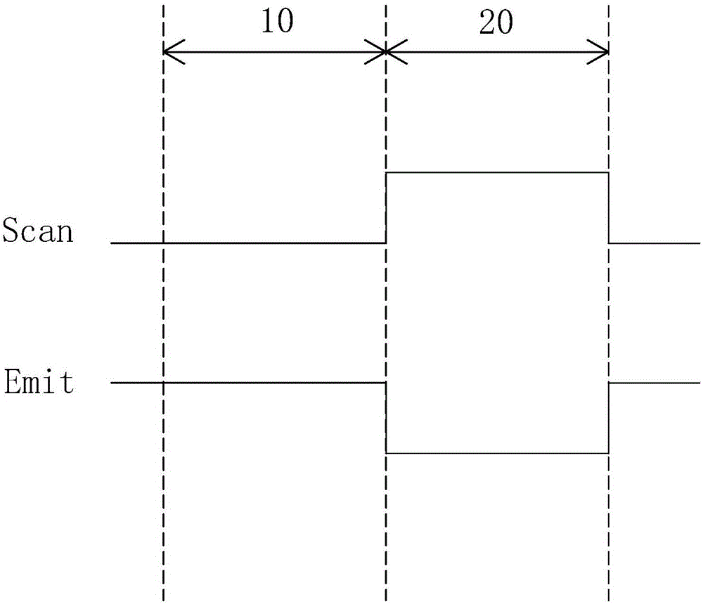
[0060] In order to further illustrate the technical means adopted by the present invention and its effects, the following describes in detail in conjunction with preferred embodiments of the present invention and accompanying drawings.

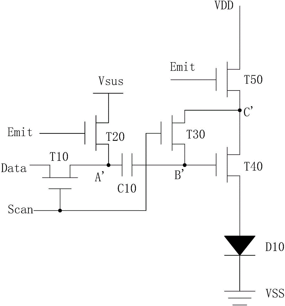
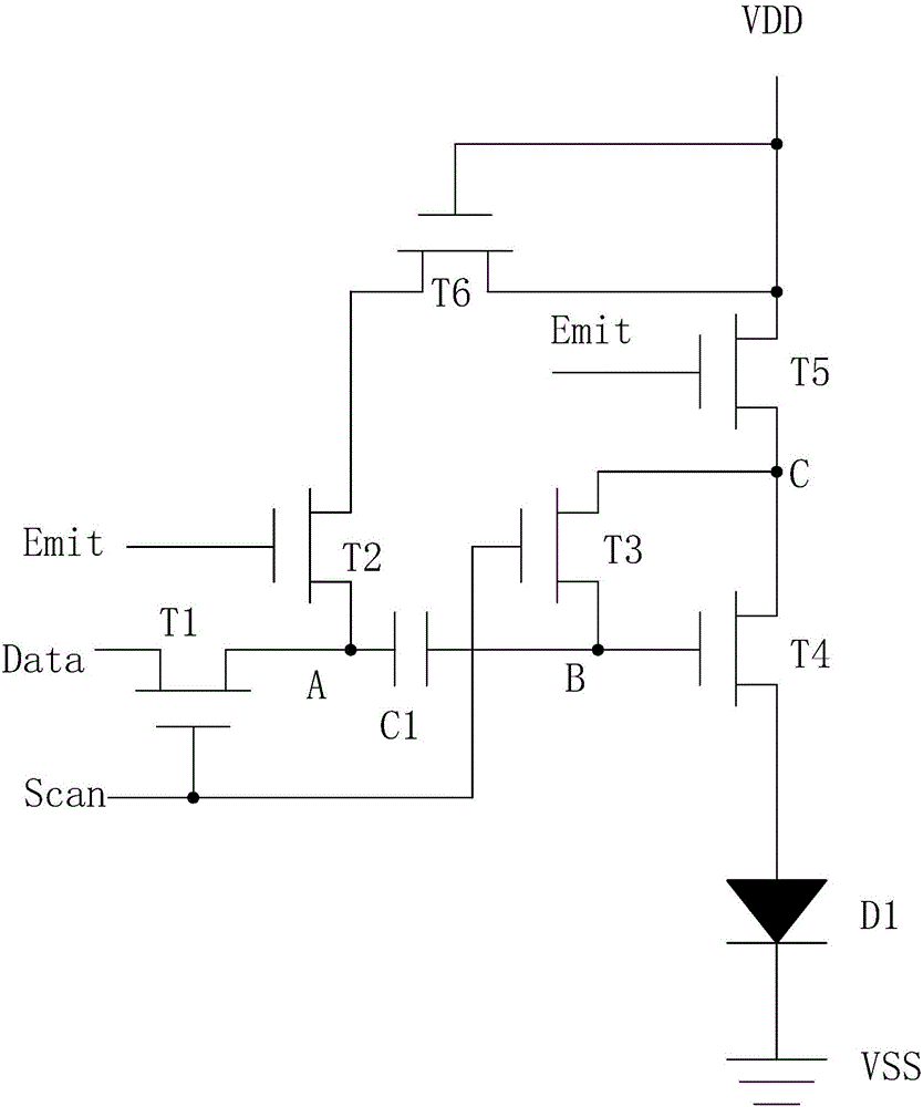
[0061] see image 3 and Figure 4 , the present invention provides an AMOLED pixel driving circuit, comprising: a first thin film transistor T1, a second thin film transistor T2, a third thin film transistor T3, a fourth thin film transistor T4, a fifth thin film transistor T5, a sixth thin film transistor T6, a A capacitor C1, and an organic light emitting diode D1.

[0062] The gate of the first thin film transistor T1 is connected to the scanning signal Scan, the source is connected to the data signal Data, and the drain is electrically connected to the first node A; the gate of the second thin film transistor T2 is connected to the light emitting signal Emit, and the source is electrically connected to the first node A. Connect the sourc...


PUM


Abstract

The invention provides an AMOLED pixel driving circuit and a pixel driving method. The AMOLED pixel driving circuit is of a 6T1C (six thin-film transistors and one capacitor) structure. The gate and the drain of a sixth thin-film transistor (T6) are short-circuited, and are connected with a positive supply voltage (VDD) to form a diode. The difference between the voltage output by the sixth thin-film transistor (T6) (namely, the positive supply voltage (VDD)) and the threshold voltage of the sixth thin-film transistor (T6) is used as a reference signal voltage. The reference signal voltage is written into a first node (A) in the driven light emitting stage to make compensation for the threshold voltage shift of a fourth thin-film transistor (T4) (namely, a driving thin-film transistor). There is no need to set a reference signal voltage separately. When the AMOLED pixel driving circuit is applied to a display panel, the number of input points of reference signal voltage is increased, the loss of reference signals in the transmission process can be reduced, the threshold voltage compensation effect can be ensured, the number of wires inside the panel can be reduced, the possibility of possible short circuit in the process can be reduced, and the yield of the panel can be improved effectively.

Description

technical field [0001] The invention relates to the field of display technology, in particular to an AMOLED pixel driving circuit and a pixel driving method. Background technique [0002] Organic light emitting diode (Organic Light Emitting Display, OLED) display device has self-illumination, low driving voltage, high luminous efficiency, short response time, high definition and contrast, nearly 180° viewing angle, wide operating temperature range, and can realize flexible display and With many advantages such as large-area full-color display, it is recognized by the industry as a display device with the most potential for development. [0003] OLED display devices can be divided into passive matrix OLED (Passive Matrix OLED, PMOLED) and active matrix OLED (Active Matrix OLED, AMOLED) two categories according to the driving method, namely direct addressing and thin film transistor (Thin Film Transistor, TFT) matrix addressing two types. Among them, AMOLED has pixels arrang...

Claims


Application Information

Patent Timeline
Patent Type & Authority Applications(China)
IPC IPC(8): G09G3/3225G09G3/3258
CPCG09G3/3225G09G3/3258G09G2320/04
Inventor 聂诚磊
Owner TCL CHINA STAR OPTOELECTRONICS TECH CO LTD
Why Eureka
Try Eureka