Eureka AIR delivers breakthrough ideas for toughest innovation challenges, trusted by R&D personnel around the world.

Composite electronic component and its preparation method

A technology of electronic components and electrode layers, applied in the direction of electrical components, circuits, capacitors, etc., can solve problems such as low placement efficiency, unfavorable miniaturization of the whole machine, and multi-circuit space

Active Publication Date: 2019-03-22
GUANGDONG FENGHUA ADVANCED TECH HLDG
View PDF4 Cites 0 Cited by
  • Summary
  • Abstract
  • Description
  • Claims
  • Application Information

AI Technical Summary

Problems solved by technology

In many circuit applications, when it is necessary to use a circuit with a series structure of resistors and capacitors, discrete components are generally used, that is, resistors are mounted outside the capacitors, and the mounting efficiency is low, forming a single resistor and a single capacitor, which takes up more circuits. Space is not conducive to the miniaturization of the whole machine

Method used


Image

  • Composite electronic component and its preparation method
  • Composite electronic component and its preparation method
  • Composite electronic component and its preparation method

Examples


preparation example Construction

[0073] The flowchart of the preparation method of the composite electronic component of one embodiment is as follows Figure 17 As shown, the following steps S110-S140 are included.

[0074] S110, providing a ceramic body.

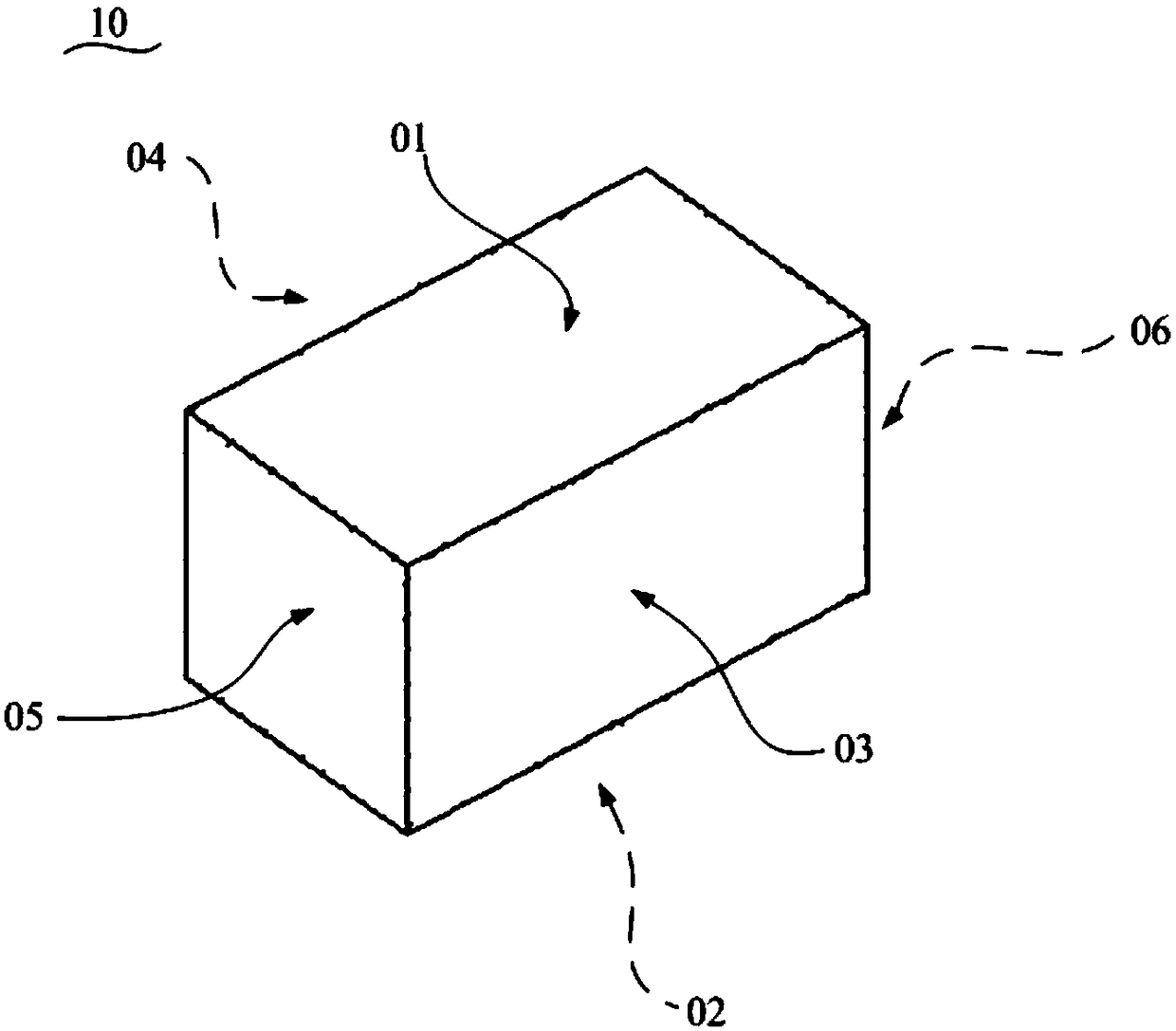
[0075] Wherein, the ceramic body is a cuboid, and the ceramic body has a first main surface and a second main surface opposite to each other, a first side surface and a second side surface opposite to each other, and a first end surface and a second end surface opposite to each other. The inside of the ceramic body is filled with a ceramic medium, and a plurality of first electrode layers and a plurality of second electrode layers are interspersed in the ceramic medium, and the first electrode layers and the second electrode layers are alternately stacked, and the first electrode layers are on the second electrode layers The projection of has an overlapping portion with the second electrode layer. A ceramic medium is filled between the first electrode la...

Embodiment 1

[0121] Preparation of composite electronic components

[0122] 1) Preparation of a ceramic body: ceramic powder, a binder and an organic solvent are mixed to obtain a ceramic slurry, and a plurality of ceramic dielectric films are formed by casting the ceramic slurry as a raw material. Wherein, the ceramic slurry includes 10 parts of ceramic powder, 4 parts of binder and 5 parts of organic solvent in parts by mass. The ceramic powder is barium titanate ceramics, the binder is polyvinyl butyral, and the organic solvent is a mixed solvent of toluene and ethanol with a ratio of parts by mass of 1:1. The electrode paste is printed on a plurality of ceramic dielectric films to respectively obtain a ceramic dielectric film printed with a first electrode layer and a ceramic dielectric film printed with a second electrode layer. The screen pattern of the first electrode layer and the second electrode layer is as Figure 19 As shown, the shaded part indicates where the electrode past...

Embodiment 2

[0128] The preparation method of the composite electronic component of this embodiment is similar to that of Embodiment 1, the difference is that in the preparation of the ceramic body, the electrode paste is printed on a plurality of ceramic dielectric films, and the ceramic dielectric film and the ceramic dielectric film printed with the first electrode layer are respectively obtained. In the operation of printing the ceramic dielectric film with the second electrode layer, the screen pattern of the first electrode layer and the second electrode layer is screen printed as Figure 20 As shown, the shaded part indicates where the electrode paste is printed. When the side electrodes are formed on the ceramic body, the first electrode layer is electrically connected to the first connection electrode and the second connection electrode, and the second electrode layer is electrically connected to the third connection electrode and the fourth connection electrode.

[0129] The spec...


PUM


Abstract

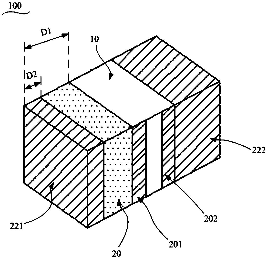
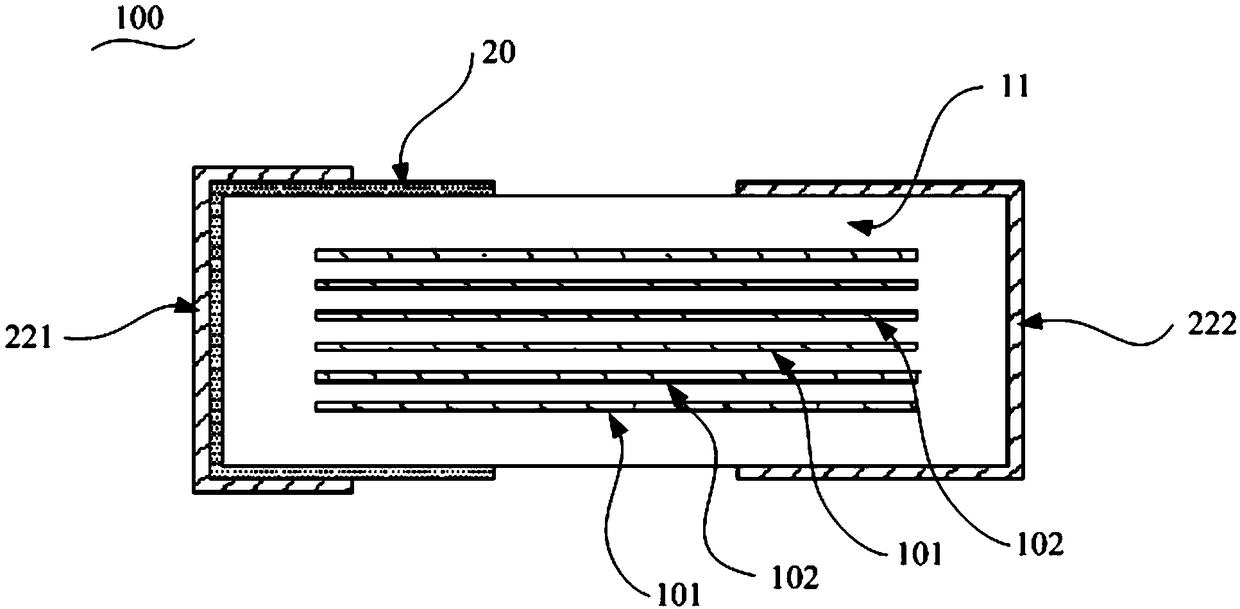
The invention discloses a composite electronic component and a preparation method thereof. According to the composite electronic component, a resistance layer is attached to at least one surface in a first end face and a second end face of a ceramic body, the resistance layer is electrically connected with at least one of a first side electrode and a second side electrode, each first electrode layer in the ceramic body is electrically connected with the first side electrode, and each second electrode layer is electrically connected with the second side electrode, so that a structure with a capacitor and a resistor connected in series is formed. The capacitor and the resistor are integrated in a single component, and thus the size is relatively small.

Description

technical field [0001] The invention relates to the technical field of electronic components, in particular to a composite electronic component and a preparation method thereof. Background technique [0002] Capacitors can be used for direct traffic isolation, filtering and energy storage, etc., and have a wide range of applications in power transmission, power distribution, and power consumption. In many circuit applications, when it is necessary to use a circuit with a series structure of resistors and capacitors, discrete components are generally used, that is, resistors are mounted outside the capacitors, and the mounting efficiency is low, forming a single resistor and a single capacitor, which takes up more circuits. Space is not conducive to the miniaturization of the whole machine. Contents of the invention [0003] Based on this, it is necessary to provide a composite electronic component with a smaller size and a preparation method thereof. [0004] A composite...

Claims


Application Information

Patent Timeline
Patent Type & Authority Patents(China)
IPC IPC(8): H01G4/40H01G4/00
CPCH01G4/00H01G4/40
Inventor 陆亨李江竹卓金丽安可荣杨晓东伍尚颖谢忠
Owner GUANGDONG FENGHUA ADVANCED TECH HLDG
Why Eureka
Eureka Blog
Learn More