Metal oxide semiconductor field effect transistor based on multi-grid structure and preparation method thereof
A metal oxide half-field and multiple gate technology, which is applied in semiconductor/solid-state device manufacturing, semiconductor devices, electrical components, etc., can solve the problems of reduced operating current and difficulty in meeting usage requirements, and achieves maintaining operating current and suppressing collapse Phenomenon, the effect of uniform electric field distribution
- Summary
- Abstract
- Description
- Claims
- Application Information
AI Technical Summary
Problems solved by technology
Method used
Image
Examples
Embodiment 1
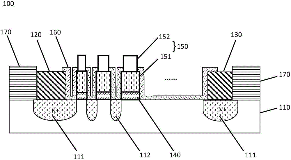
[0035] refer to figure 1 , the metal oxide semiconductor field effect transistor 100 of the present embodiment comprises a P-based N-channel substrate 110, the substrate 110 is a P-type silicon semiconductor, and two N+ regions 111 are formed by N-type heavy doping and are located between the two N+ regions. Several N-type doped regions 112 between the regions 111. The sources 120 and 130 are respectively drawn above the two N+ regions 111, and a number of oxide layers 140 are arranged at intervals between the source electrodes 120 and the drain electrodes 130, and sub-gates 150 are arranged one by one above the oxide layers 140, that is, the sub-gates The electrodes 150 are arranged at intervals from the source 120 to the drain 130 to form a multiple gate structure, and the gaps between adjacent sub-gates 150 correspond to the N-type doped regions 112 one-to-one. Each sub-gate 150 includes a polysilicon layer 151 and an electrode layer 152 disposed above the polysilicon laye...
Embodiment 2
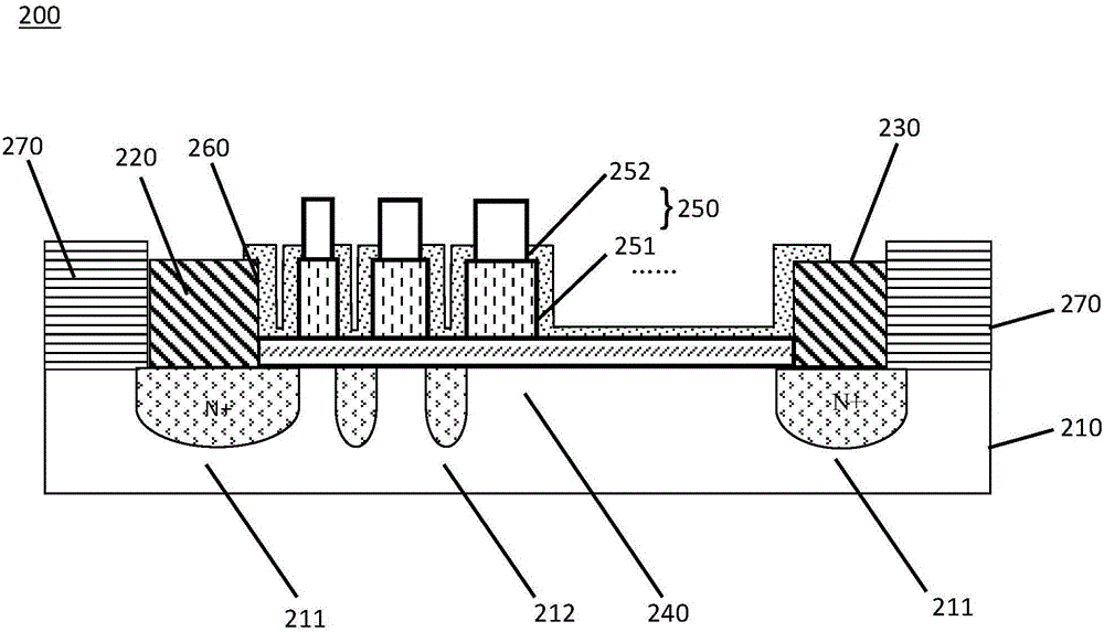
[0047] refer to figure 2 , the metal oxide semiconductor field effect transistor 200 of the present embodiment comprises a substrate 210 of a P-based N-channel, the substrate 210 is a P-type silicon semiconductor, and two N+ regions 211 are formed by N-type heavy doping and are located between the two N+ regions. Several N-type doped regions 212 between the regions 211. The sources 220 and 230 are respectively drawn above the two N+ regions 211, an oxide layer 240 is formed between the source 220 and the drain 230, and a plurality of sub-gates 250 are arranged above the oxide layer 240, and these sub-gates 250 are formed from the source 220 to the drain 230. The drain electrodes 230 are arranged at intervals to form a multiple gate structure, and the gaps between adjacent sub-gates 250 correspond to the N-type doped regions 212 one-to-one. Each sub-gate 250 includes a polysilicon layer 251 and an electrode layer 252 disposed above the polysilicon layer 251 . A passivation l...
PUM
| Property | Measurement | Unit |
|---|---|---|
| Length | aaaaa | aaaaa |
| Thickness | aaaaa | aaaaa |
| Thickness | aaaaa | aaaaa |
Abstract
Description
Claims
Application Information
 - R&D Engineer
- R&D Manager
- IP Professional
- Industry Leading Data Capabilities
- Powerful AI technology
- Patent DNA Extraction
Browse by: Latest US Patents, China's latest patents, Technical Efficacy Thesaurus, Application Domain, Technology Topic, Popular Technical Reports.
© 2024 PatSnap. All rights reserved.Legal|Privacy policy|Modern Slavery Act Transparency Statement|Sitemap|About US| Contact US: help@patsnap.com


