STI diode for ESD protection

A diode and fin technology, applied in the field of STI diodes, can solve the problems of high expansion resistance, high current non-uniformity, damage, etc., and achieve the effect of improving area efficiency, good uniformity, and small on-resistance

Active Publication Date: 2017-04-05
SEMICON MFG INT (SHANGHAI) CORP +1
View PDF3 Cites 6 Cited by
  • Summary
  • Abstract
  • Description
  • Claims
  • Application Information

AI Technical Summary

Problems solved by technology

Small silicide regions defined by Li produce higher spreading resistance and hi...

Method used


Image

  • STI diode for ESD protection
  • STI diode for ESD protection
  • STI diode for ESD protection

Examples


Embodiment 1

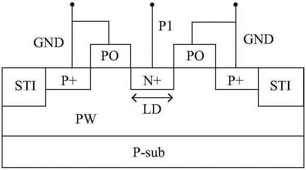
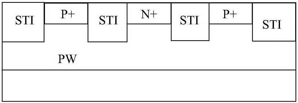
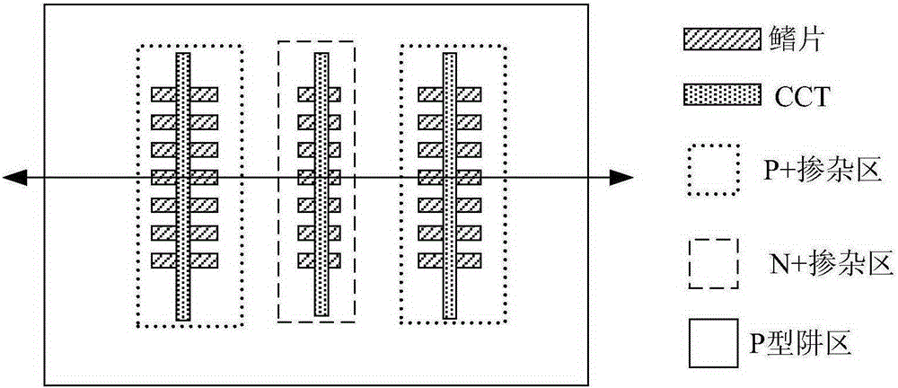
[0039] Below, refer to Figure 3A and Figure 3B An STI diode for ESD protection proposed by an embodiment of the present invention will be described. in, Figure 3A It is a plane layout diagram of a STI diode for ESD protection according to an embodiment of the present invention; Figure 3B for correspondence Figure 3A A schematic cross-sectional view of an STI diode used for ESD protection according to an embodiment of the present invention obtained by the hatching line.

[0040] Exemplarily, an STI diode for ESD protection according to an embodiment of the present invention includes:

[0041] The semiconductor substrate 100, specifically, the semiconductor substrate 100 may be at least one of the materials mentioned below: silicon, silicon-on-insulator (SOI), silicon-on-insulator (SSOI), and germanium-on-insulator Silicon (S-SiGeOI), silicon germanium on insulator (SiGeOI) and germanium on insulator (GeOI), etc.

[0042] A well region with a first conductivity type i...


PUM


Abstract

The invention provides an STI diode for ESD protection, and relates to the technical field of semiconductors. The diode comprises a semiconductor substrate, wherein the interior of the semiconductor substrate is provided with a well region of a first conductive type; a plurality of first fins which are located on the semiconductor substrate and extend in a first direction, wherein the interior of each first fin is provided with a first doped region of a first conductive type, which extends in the first direction; a plurality of second fins which are located among the first fins and extend in the first direction, wherein the interior of each second fin is provided with a second doped region of a second conductive type, which extend in the first direction; and an isolation structure which is formed on the semiconductor substrate between the first fins and the second fins. The diode provided by the invention improves the area efficiency of a device, enables the uniformity of metal silicide to be better, and enables an ESD device to be higher in secondary breakdown current and smaller in on resistance (Ron).

Description

technical field [0001] The invention relates to the technical field of semiconductors, in particular to an STI diode used for ESD protection. Background technique [0002] With the continuous development of semiconductor technology, the improvement of integrated circuit performance is mainly achieved by continuously shrinking the size of integrated circuit devices to increase its speed. Currently, the semiconductor industry has progressed to nanotechnology process nodes in pursuit of high device density, high performance, and low cost. However, this progressive trend has a negative impact on the reliability of end products: In the field of semiconductor technology, the electrostatic discharge (ESD) phenomenon is a major threat to integrated circuits, which can break down integrated circuits and semiconductor components, causing Component aging reduces production yield. Therefore, with the continuous reduction of the size of the semiconductor manufacturing process, the ESD ...

Claims


Application Information

Patent Timeline
IPC IPC(8): H01L29/861H01L27/02
CPCH01L27/0255H01L29/861
Inventor 李勇
Owner SEMICON MFG INT (SHANGHAI) CORP
Why Eureka
Try Eureka