Method for measuring surface morphology to detect internal defects of interlayer of double-layer or multi-layer film

A technology for measuring surfaces and multilayer films. It is used in optical testing for flaws/defects, measuring devices, and material analysis by optical means. low threshold effect

Active Publication Date: 2017-04-26
HARBIN INST OF TECH
View PDF5 Cites 1 Cited by
  • Summary
  • Abstract
  • Description
  • Claims
  • Application Information

AI Technical Summary

Problems solved by technology

[0003] In order to solve the problems of destructive processing, time-consuming, and high cost in the preparation and testing of existing thin-film devices, microelectronics, and microelectronic machinery, the invention provides a method for measuring surface topography to detect double-layer and multi-layer thin films. The method of internal defects between layers, using the phenomenon of morphology changes on the surface of the film before and after aging, thermal cycle or mechanical cycle due to the appearance of internal defects to identify the location and size of the defects

Method used


Image

  • Method for measuring surface morphology to detect internal defects of interlayer of double-layer or multi-layer film
  • Method for measuring surface morphology to detect internal defects of interlayer of double-layer or multi-layer film
  • Method for measuring surface morphology to detect internal defects of interlayer of double-layer or multi-layer film

Examples


specific Embodiment approach 1

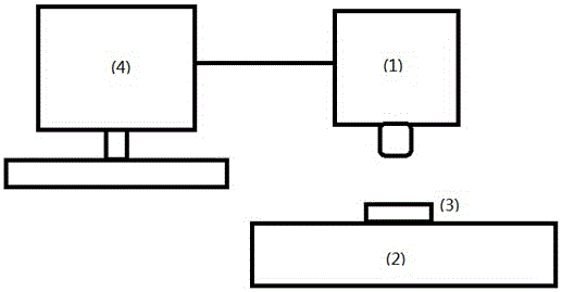
[0030] Specific implementation mode one: as figure 1 As shown, this embodiment provides a device for measuring surface topography to detect internal defects between layers of double-layer and multi-layer thin films. , the specific detection steps are as follows:

[0031] 1. Place the tested part 3 on the low-temperature heating platform 2, the surface topography detection device 1 is located above the tested part 3, and record the placement position of the tested part 3 on the low-temperature heating platform;

[0032] 2. Adjust and record various parameters of the surface topography detection device 1, and use this as a reference parameter to detect the tested part 3;

[0033] 3. Set the low-temperature heating platform 2 to room temperature, measure and record the surface morphology of the tested part 3;

[0034] 4. Set the low-temperature heating platform 2 for constant temperature heating, measure and record the surface morphology of the tested part 3, and turn off the l...

specific Embodiment approach 2

[0050] Specific implementation mode 2: This implementation mode provides a method for measuring surface topography to detect internal defects between double-layer and multi-layer film layers, and the specific implementation steps are as follows:

[0051] 1. The tested part is composed of nickel film and substrate;

[0052] 2. Use an optical 3D surface topography detection device for measurement, and its parameters are as follows: 5x objective lens, 1.76μm×1.76μm pixel size, 410nm vertical resolution, 2.2μm lateral resolution, and the ambient temperature of the lens is required to be 45°C ;

[0053] 3. Place the tested part on the low-temperature heating platform, the surface topography detection device is located above the tested part, and record the placement position of the tested part on the low-temperature heating platform;

[0054] 4. Set the low-temperature heating platform to room temperature, and use the surface topography detection device to measure the 3D topography...


PUM

PropertyMeasurementUnit
thicknessaaaaaaaaaa
thicknessaaaaaaaaaa

Abstract

The invention discloses a method for measuring surface morphology to detect internal defects of the interlayer of a double-layer or multi-layer film, belonging to the technical fields of microelectronics and microelectronic machinery manufacturing. To overcome the problems of destructive processing, long operation time, high cost and the like in preparation and detection of thin-film devices, microelectronic devices, microelectronic machines and other devices, the invention provides the method for measuring surface morphology to detect internal defects of the interlayer of a double-layer or multi-layer film. The method identifies the positions and sizes of the defects according to morphological changes of the surface of the film before and after ageing, heat cycle or mechanical cycle caused by the internal defects. The method has the characteristics of rapidness, no destruction, instantaneity and low detection cost. When the method is applied to information electronic manufacturing fields like microelectronics and microelectronic machinery, manufacturing cost and testing cost are greatly reduced and quality is improved, so the method has good application prospects in the above fields and in the field of manufacturing of structures of a same kind.

Description

technical field [0001] The invention belongs to the technical field of microelectronics and microelectronic machinery manufacturing, and relates to a novel defect detection method, in particular to a method for measuring surface topography and detecting internal defects between double-layer and multi-layer film layers. Background technique [0002] Multilayer thin film is the basic structure of thin film devices, microelectronic devices, microelectronic machinery (MEMS), etc. in the field of information electronics manufacturing. It is characterized by double or multi-layer films and thin substrates made by evaporation, sputtering, chemical deposition, spin coating, bonding and other processes. During the preparation process, there will be tiny defects between the membrane and the membrane due to various reasons, such as air bubbles, delamination, cracks, slag inclusions, foreign matter and so on. In order to control the quality of multi-layer thin films and ensure the firm...

Claims


Application Information

Patent Timeline
Patent Type & Authority Applications(China)
IPC IPC(8): G01N21/95
CPCG01N21/8422G01N21/95G01N2021/8438
Inventor 王晓婷王春青
Owner HARBIN INST OF TECH
Why Eureka
Try Eureka