Method for preparing SiGe-based plasma pin diode for reconstructing holographic antennas
A holographic antenna and plasma technology, which is applied to devices, antennas, and antenna components that make the antennas work in different bands at the same time, can solve problems such as incompatibility, uneven doping concentration, and influence on solid-state plasma concentration, and improve the Enhanced performance, controllability
- Summary
- Abstract
- Description
- Claims
- Application Information
AI Technical Summary
Problems solved by technology
Method used
Image
Examples
Embodiment 1
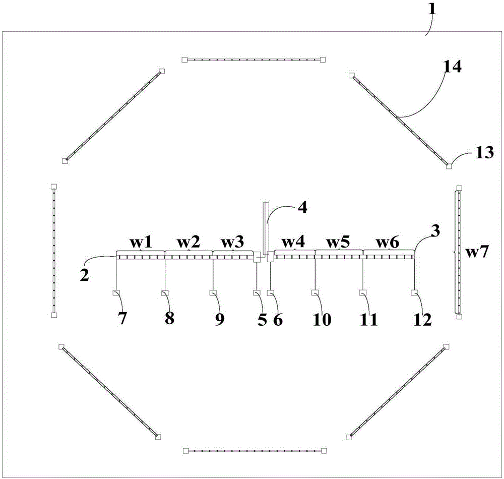
[0054] This embodiment provides a method for preparing a SiGe-based plasmonic pin diode used for a reconfigurable holographic antenna, and the SiGe-based plasmonic pin diode is used for making a reconfigurable holographic antenna. See figure 1 , figure 1 It is a structural schematic diagram of a reconfigurable holographic antenna according to an embodiment of the present invention. The reconfigurable holographic antenna includes: a SiGeOI semiconductor substrate (1); a first antenna fabricated on the SiGeOI semiconductor substrate (1) Arm (2), second antenna arm (3), coaxial feeder (4) and holographic ring (14); wherein, the first antenna arm (2) and the second antenna arm (3) include distributed SiGe-based plasma pin diode strings of equal length on both sides of the coaxial feeder (4), the holographic ring (14) includes a plurality of SiGe-based plasma pin diode strings (w7).
[0055] The antenna arm of the reconfigurable holographic antenna provided by the embodiment of t...
Embodiment 2
[0100] See Figure 5a-Figure 5s , Figure 5a-Figure 5s It is a schematic diagram of the preparation method of another SiGe-based plasmonic pin diode according to the embodiment of the present invention. On the basis of the first embodiment above, to prepare a SiGe-based solid-state plasmonic pin with a channel length of 22 nm (the length of the solid-state plasma region is 100 microns) Taking a diode as an example to describe in detail, the specific steps are as follows:
[0101] Step 1, substrate material preparation steps:
[0102] (1a) if Figure 5a As shown, the SiGeOI substrate 101 with (100) orientation is selected, the doping type is p-type, and the doping concentration is 10 14 cm -3 , the thickness of the top layer SiGe is 50 μm;
[0103] (1b) if Figure 5b As shown, the chemical vapor deposition (Chemical vapor deposition, CVD) method is used to deposit a layer of first SiO with a thickness of 40 nm on SiGe. 2 layer 201;
[0104] (1c) Deposit a layer of first...
Embodiment 3
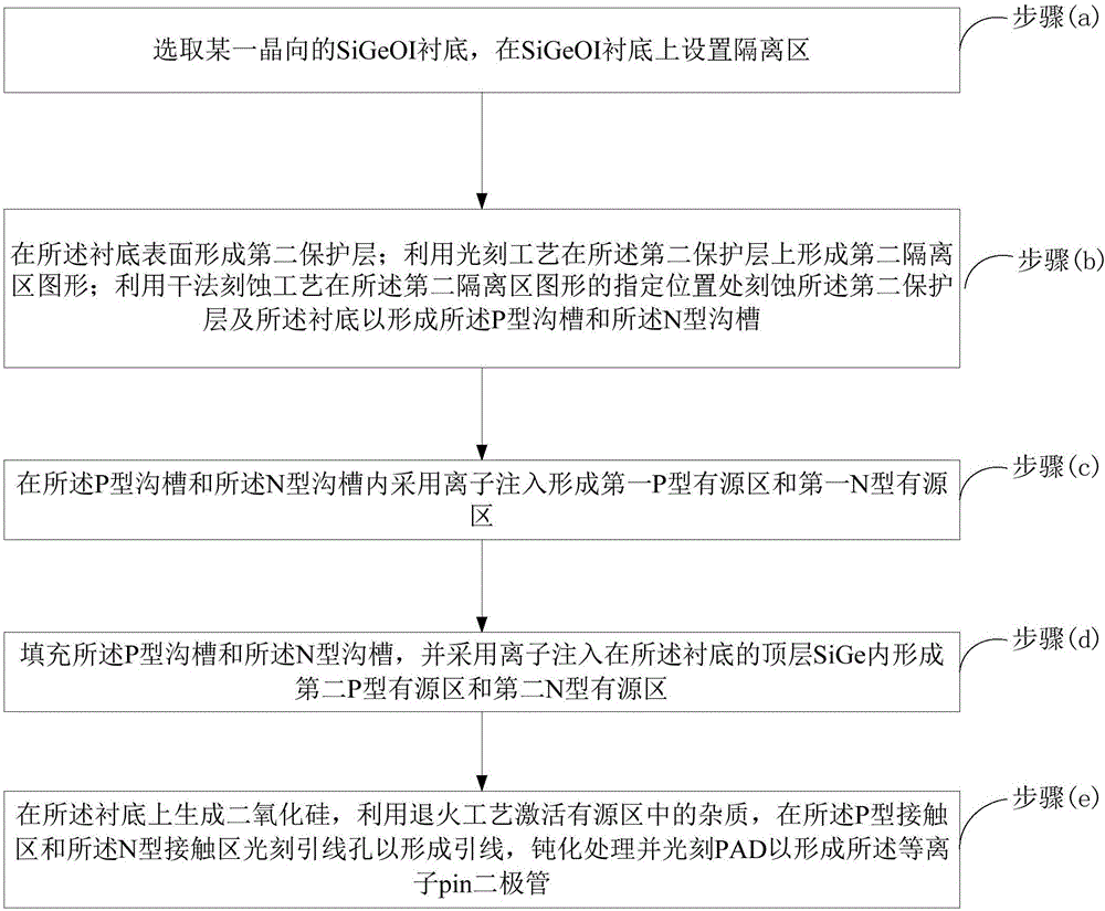
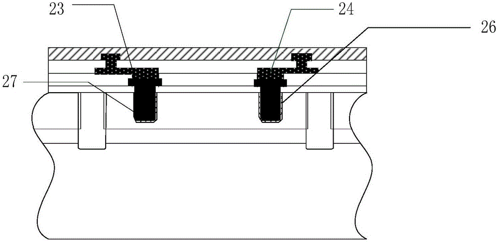
[0133] Please refer to Figure 6 , Figure 6 It is a schematic diagram of the device structure of another SiGe-based plasmonic pin diode according to an embodiment of the present invention. The plasmonic pin diode employs the above as figure 2 The preparation method shown is made, specifically, the plasma pin diode is prepared and formed on the SiGeOI substrate 301, and the P region 305, the N region 306 of the pin diode and the laterally located between the P region 305 and the N region 306 The I regions are located in the top layer SiGe302 of the substrate. Wherein, the pin diode can be isolated by STI deep trenches, that is, an isolation trench 303 is provided outside the P region 305 and the N region 306, and the depth of the isolation trench 303 is greater than or equal to the thickness of the top SiGe layer. In addition, the P region 305 and the N region 306 may respectively include a thin-layer P-type active region 307 and a thin-layer N-type active region 304 along...
PUM
 Abstract
Description
Claims
Application Information


