Capping layer, OLED display panel comprising capping layer and electronic device
A display panel and cover layer technology, applied in circuits, electrical components, electrical solid devices, etc., can solve problems such as unsatisfactory light extraction efficiency of devices, ensure overall light extraction efficiency, improve film formation stability and optical performance, and improve transparency. light effect
- Summary
- Abstract
- Description
- Claims
- Application Information
AI Technical Summary
Problems solved by technology
Method used
Image
Examples
preparation example Construction
[0060] Exemplary as A preparation method comprising the steps of:
[0061]
[0062] When B is selected from any one of substituted or unsubstituted C5-C10 cycloalkyl, substituted or unsubstituted C6-C30 aromatic groups with at least 2 broken bonds, it can be prepared by the following method:
[0063]
Embodiment 1
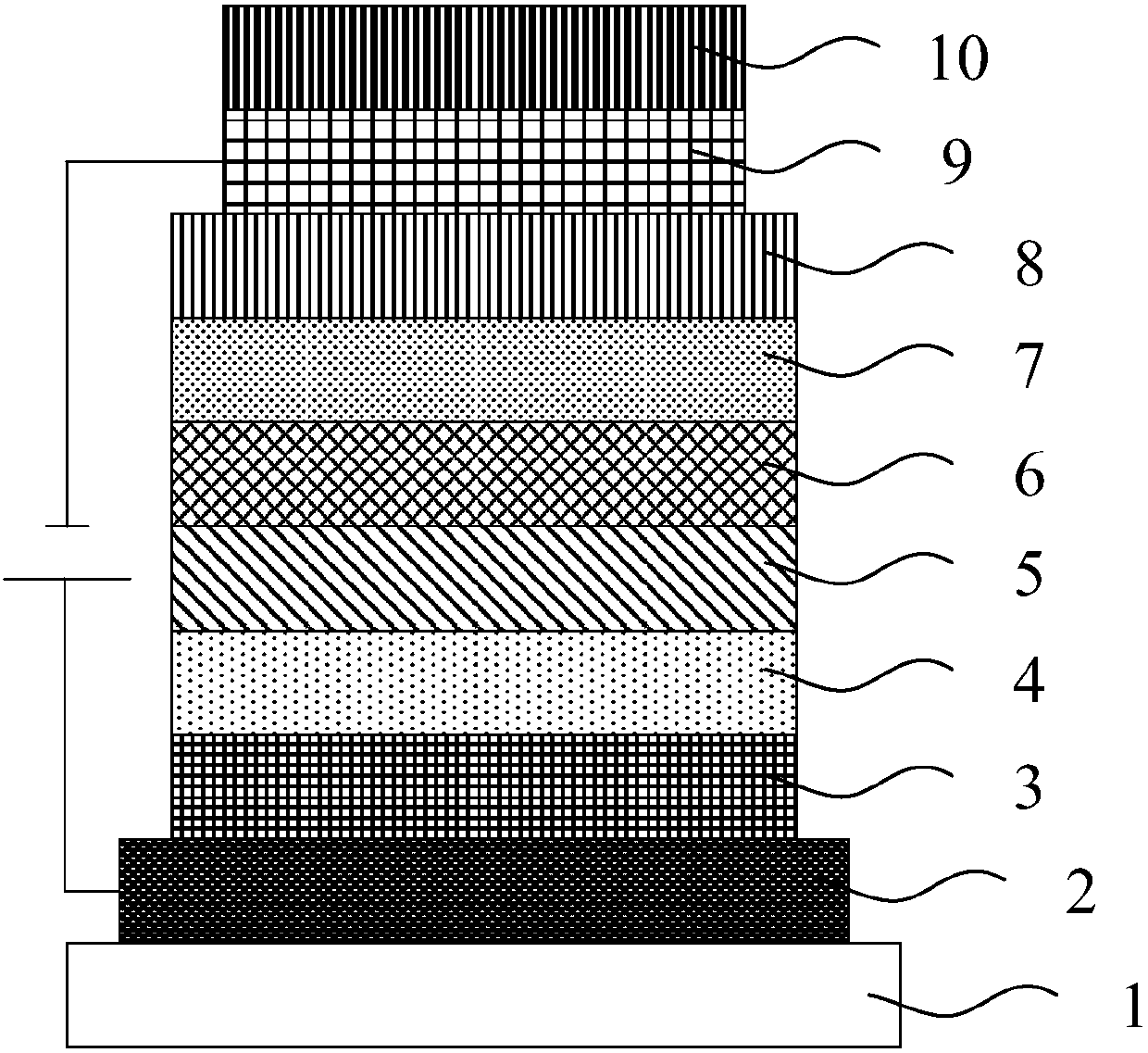
[0066] figure 1 An OLED display panel S1 is provided, including the following structure from bottom to top:
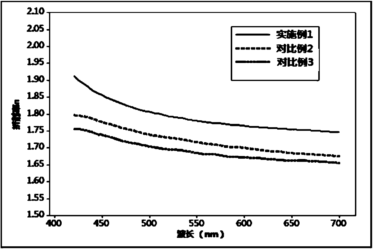
[0067] Substrate 1, silver reflective electrode (100nm), ITO electrode 2 (15nm), first hole transport layer 3 (10nm), second hole transport layer 4 (110nm), light emitting layer 6 (30nm), first electron transport layer Layer 7 (30nm), second electron transport layer 8 (5nm), magnesium-silver electrode (magnesium-silver mass ratio 9:1wt) 9 (15nm) and covering layer 10, and described covering layer is passed Obtained by evaporation, the thickness of the covering layer is 70nm, and the refractive index n of the covering layer is 450~650nm >1.76, the refractive index of 450nm, 530nm, 620nm is 1.84, 1.78, 1.76 respectively;
[0068] The first hole transport layer is (P-type dopant material) material and Doping, the mixing ratio is 5:95 (mass ratio); the second hole transport layer is Material; light-emitting layer is BD :BH Materials, 5:95; the first electron t...
Embodiment 2
[0070] The difference from Example 1 is that the material of the covering layer is The thickness of the covering layer is 70nm, and the refractive index n of the covering layer 450~650nm >1.8, the refractive indices of 450nm, 530nm, and 620nm are 1.95, 1.87, and 1.82, respectively.
PUM
 Abstract
Description
Claims
Application Information


