An intelligent junction box for eliminating pid decay and its working method
A junction box and intelligent technology, applied in electrical components, photovoltaic modules, photovoltaic power generation, etc., can solve the problems of increasing the risk factor of the system, no operator provides a satisfactory solution, and photovoltaic inverter cannot be used, etc., to reduce investment Cost and maintenance cost, elimination of PID long-term decay effect, effect of prolonging effective service life
- Summary
- Abstract
- Description
- Claims
- Application Information
AI Technical Summary
Problems solved by technology
Method used
Image
Examples
Embodiment 1
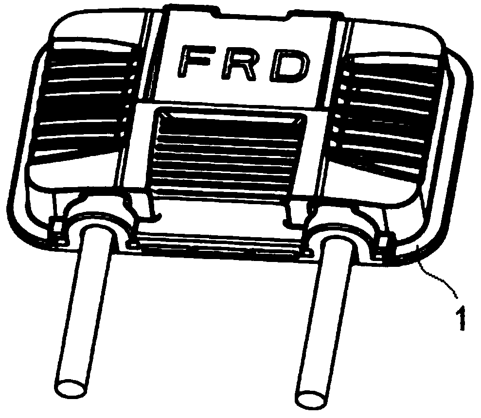
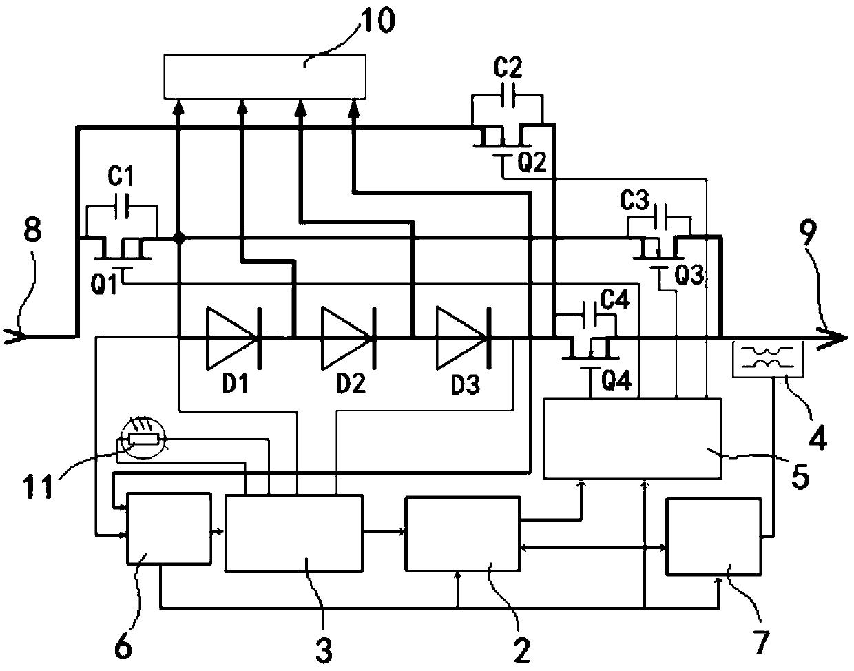
[0043] Such as figure 1 , figure 2 Shown, a kind of intelligent junction box that eliminates PID decay of the present invention comprises:
[0044] A junction box housing 1, the junction box housing 1 is a sealed junction box shell. The junction box housing 1 is an intelligent photovoltaic junction box with circuits such as voltage and current detection circuits, an output polarity switch, and a central processing unit installed inside. The interior of the junction box housing 1 is specifically equipped with a central processing unit 2, a photoelectric sampling module 3, a carrier signal coupling element 4, a switch signal drive circuit 5, a working power supply module 6, a carrier signal transceiver module 7, a negative connector 8, a positive Connector 9, multiple MOS type electronic switches and bypass diodes. Copper conductors, positive and negative output wires, cables, etc. of a conventional junction box are retained in the junction box housing 1 . The PID decay eli...
Embodiment 2
[0076] This embodiment provides a working method of an intelligent junction box that eliminates PID decay, including the following steps:
[0077] S1: The carrier signal coupling element 4 receives the carrier signal of the inversion command on the line, and sends the carrier signal to the central processing unit 2 through the carrier signal transceiver module 7 .
[0078] S2: The photoelectric sampling module 3 collects the voltage value at both ends of the bypass diode and sends the voltage value to the central processing unit 2 .
[0079] S3: The central processing unit 2 receives the carrier signal and the voltage value, analyzes the carrier signal and the voltage value, and if the carrier signal conforms to the agreed format, then directly enters step S4, otherwise, judges the Whether the voltage value exceeds the threshold value, if the voltage value exceeds the threshold value, enter step S4, if the voltage value does not exceed the threshold value, then maintain the cu...
PUM
 Abstract
Description
Claims
Application Information

