Silicon wafer cleaning agent

A technology of silicon wafer cleaning agent and alkali agent, which is applied in the directions of detergent compounding agent, detergent composition, surface active detergent composition, etc., can solve the problems of surface corrosion of silicon wafer, appearance of spots, unsatisfactory cleaning effect, etc.

Inactive Publication Date: 2017-05-17
DEQING LIJING ENERGY TECH CO LTD
View PDF4 Cites 12 Cited by
  • Summary
  • Abstract
  • Description
  • Claims
  • Application Information

AI Technical Summary

Problems solved by technology

Due to the formula and other reasons, the conventional silicon wafer cleaning agent takes a long time to clean, generally takes 600-1200s, and the cleaning effect is not ideal, the surface of the silicon wafer is severely corroded, and spots may appear

Method used


Image

  • Silicon wafer cleaning agent
  • Silicon wafer cleaning agent

Examples


Embodiment 1-4

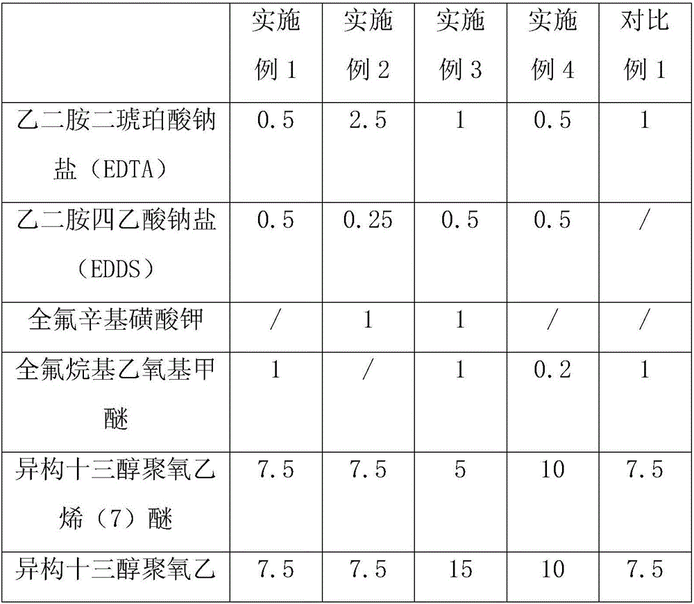
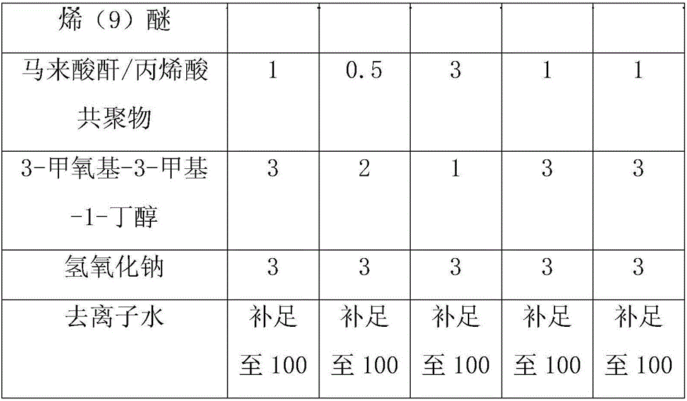
[0022] According to Table 1, add the raw materials into deionized water in sequence, raise the temperature to 40-50° C., stir evenly, and cool to room temperature to prepare the silicon wafer cleaning agent.

[0023] Table 1 silicon wafer cleaning agent formula (the numerical value in the table is the weight percent of this component)

[0024]

[0025]

[0026] Silicon wafers were cleaned in Examples 1-4 and Comparative Example 1 above. The specific cleaning method is as follows: add 10g of the cleaning agents of Examples 1-4 and Comparative Example 1 into a cleaning tank filled with 240g of deionized water, mix well, then immerse the silicon wafer in the cleaning tank, and the cleaning time is 50°C , the cleaning temperature is 480s.

[0027] The silicon wafers washed in Examples 1-4 are visually smooth, colorless, and have no obvious residual stains.


PUM


Abstract

The invention belongs to the technical field of monocrystalline silicon wafer appliance, and particularly relates to a silicon wafer cleaning agent. The invention discloses the silicon wafer cleaning agent characterized by comprising the following components by weight: 0.5-2% of a metal chelating agent, 0.2-2% of a fluorocarbon surfactant, 5-20% of fatty alcohol polyoxyethylene ether, 0.5-3% of polymer additives, 0.5-2% of a co-solvent, 1-5% of an alkaline agent and the balance of water. The beneficial effects of the invention are that the compound metal chelating agent of EDTA and EDDS can effectively chelate and remove metal ions on the surface of a silicon wafer in the process of cleaning the silicon wafer, especially Cu, Fe, Zn and other ions having relatively great influence on the photoelectric conversion efficiency of the silicon wafer at a later stage; the cleaning agent has no irritating smell, has good oil stain removing effect on the silicon wafer, and does not cause serious corrosion to the silicon wafer.

Description

technical field [0001] The invention belongs to the technical field of single crystal silicon wafer appliances, in particular to a silicon wafer cleaning agent. Background technique [0002] Silicon wafer processing mostly adopts multi-wire cutting technology. During this process, silicon carbide abrasives cut silicon wafers, which will form organic contamination and metal ion contamination on the surface of silicon wafers. Residues of metal ion pollutants such as copper Cu, iron Fe, zinc Zn, etc. will affect the quality of the gate film formed by subsequent oxidation on the surface of the silicon wafer, resulting in easy leakage of components, low yield, and poor reliability. It can be seen that the removal of metal ions on the surface of the silicon wafer has a great impact on the efficacy of its subsequent components. At the same time, oxidation of the silicon wafer surface, fingerprint contamination, etc. will also affect its photoelectric conversion efficiency. Theref...

Claims


Application Information

Patent Timeline
Patent Type & Authority Applications(China)
IPC IPC(8): C11D1/825C11D1/831C11D3/20C11D3/33C11D3/37C11D3/60
CPCC11D1/831C11D1/004C11D1/721C11D1/8255C11D3/2068C11D3/33C11D3/3765C11D11/0023
Inventor 姜翰钦
Owner DEQING LIJING ENERGY TECH CO LTD
Why Eureka
Try Eureka