

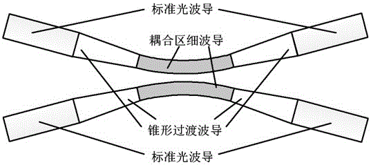
High-efficiency coupling structure among silicon-based optical waveguides and manufacturing method thereof
A silicon-based optical waveguide and coupling structure technology, applied in the direction of coupling of optical waveguides, can solve the problems of low reliability, large volume, and high power consumption, and achieve the effects of reducing process errors, improving process tolerance, and small additional loss
- Summary
- Abstract
- Description
- Claims
- Application Information
AI Technical Summary
Problems solved by technology
Method used
Image

Examples
Embodiment 1
[0034] The method of fabricating an efficient coupling structure between silicon-based optical waveguides includes the following steps:
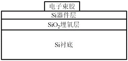
[0035] 1) Coat the electron beam glue on the silicon material on the insulator. The electron beam glue adopts ZEP520A, the glue thickness is 350 nanometers, and the coupled waveguide pattern is directly written by electron beam lithography, and the electron beam glue mask is made by development. The cross-sectional view of the produced photoresist waveguide etching mask is as follows figure 2 Shown
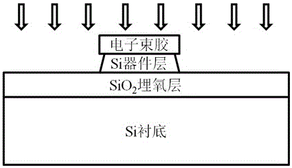
[0036] 2) Using photoresist as an etching mask, use inductively coupled plasma to etch a trapezoidal silicon-based optical waveguide, such as image 3 Shown. The gas used for the etching of silicon is a mixture of sulfur hexafluoride and oxygen. The specific etching conditions are: sulfur hexafluoride flow rate is 5 sccm, oxygen flow rate is 3 sccm, air pressure is 0.5 pa, etching coil power is 90W, radio frequency The bias power is 5W, and the etc...
Embodiment 2
[0039] The method of fabricating an efficient coupling structure between silicon-based optical waveguides includes the following steps:
[0040] 1) Coat the electron beam glue on the silicon material on the insulator. The electron beam glue adopts ZEP520A, the glue thickness is 500 nanometers, and the coupled waveguide pattern is directly written by electron beam lithography, and the electron beam glue mask is made by development. The cross-sectional view of the produced photoresist waveguide etching mask is as follows figure 2 Shown
[0041] 2) Using photoresist as an etching mask, use inductively coupled plasma to etch a trapezoidal silicon-based optical waveguide, such as image 3 Shown. The gas used for the etching of silicon is a mixed gas of sulfur hexafluoride and oxygen. The specific etching conditions are: sulfur hexafluoride flow rate is 10 sccm, oxygen flow rate is 5 sccm, air pressure is 1.0 pa, etching coil power is 120W, radio frequency The bias power is 10W, and th...
Embodiment 3
[0044] The method of fabricating an efficient coupling structure between silicon-based optical waveguides includes the following steps:
[0045] 1) Coat the electron beam glue on the silicon material on the insulator. The electron beam glue adopts ZEP520A, the glue thickness is 400 nanometers, and the coupled waveguide pattern is directly written by electron beam lithography, and the electron beam glue mask is made by development. The cross-sectional view of the produced photoresist waveguide etching mask is as follows figure 2 Shown
[0046] 2) Using photoresist as an etching mask, use inductively coupled plasma to etch a trapezoidal silicon-based optical waveguide, such as image 3 Shown. The gas used for the etching of silicon is a mixture of sulfur hexafluoride and oxygen. The specific etching conditions are: sulfur hexafluoride flow rate is 8 sccm, oxygen flow rate is 4 sccm, air pressure is 0.75 pa, etching coil power is 90W, radio frequency The bias power is 8W, and the et...
PUM
 Abstract
Description
Claims
Application Information