Photonic crystal waveguide coupler for two-dimensional silicon-based terahertz frequency domain

A photonic crystal waveguide and terahertz technology, applied in the field of optical communication, can solve the problems of little research, low transmission efficiency, and no attention to structural terahertz wave transmission, etc., and achieve the effect of reducing transmission loss, flexible structure, and regular structure.

Inactive Publication Date: 2017-05-24
QINGDAO UNIV
View PDF2 Cites 8 Cited by
  • Summary
  • Abstract
  • Description
  • Claims
  • Application Information

AI Technical Summary

Problems solved by technology

[0006] However, the existing research on silicon-based photonic crystal waveguides mostly focuses on the functional units and structural design of the photonic crystal waveguide structure itself. The primary problem in the design of photonic crystal waveguides in the terahertz frequency domain is to couple free-space terahertz waves into waveguides (or optical fibers) for transmission, which is the basis for improving the efficiency and stability of terahertz systems
Because terahertz waves are difficult to couple into photonic crystal slab waveguides, many research results show that its final transmission efficiency is less than 70%, and some studies have its final transmission loss even exceed 6dB; the second is that photonic crystals are not well utilized. The slow-light characteristics of the structure combine the slow-light characteristics with reducing the transmission loss of the terahertz waveguide (or optical fiber) and realizing broadband information transmission.
Many studies have focused on the functional design of power splitters, filters and optical switches, and their theoretical and experimental results are better than traditional waveguide structures, but most structures only use the bandgap characteristics of photonic crystal structures, not only do not use photonic crystals Slow light effect characteristics, and did not pay attention to the influence of structure optimization on terahertz wave transmission

Method used


Image

  • Photonic crystal waveguide coupler for two-dimensional silicon-based terahertz frequency domain
  • Photonic crystal waveguide coupler for two-dimensional silicon-based terahertz frequency domain
  • Photonic crystal waveguide coupler for two-dimensional silicon-based terahertz frequency domain

Examples


Embodiment 1

[0043] Example 1: Quadrilateral array coupled cavity terahertz waveguide based on (3+1+3) microcavities

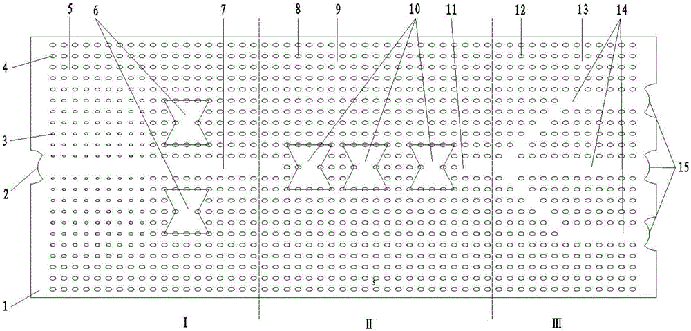
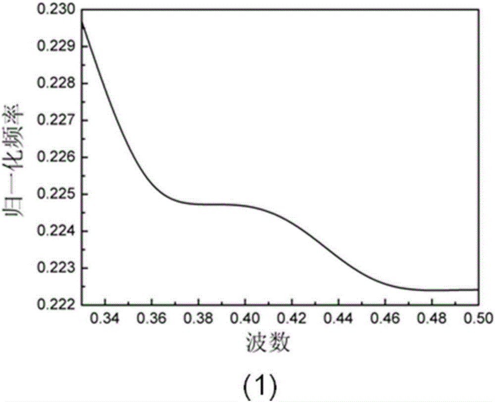
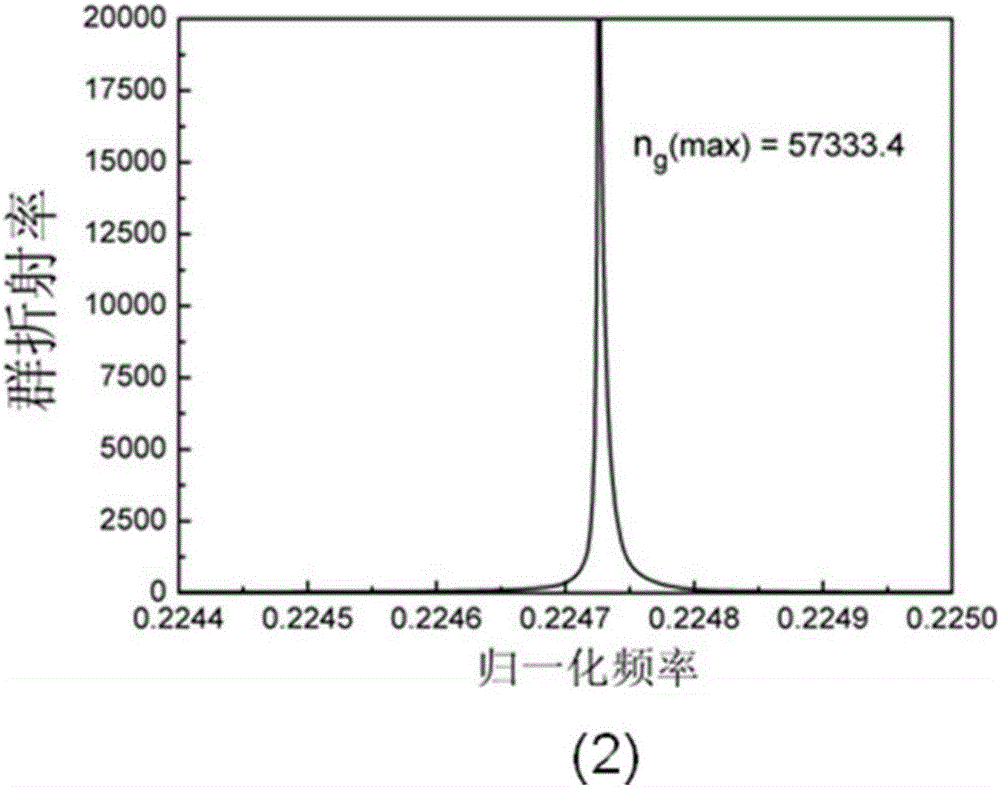
[0044] The structure of the photonic crystal waveguide coupler in the two-dimensional silicon-based terahertz frequency domain described in this embodiment is as follows: figure 1 As shown, the frequency f of the terahertz wave emitted by the external wave source is f=1THz=10 12 Hz, its wavelength is λ=300μm, the terahertz wave emitted by the wave source first reaches the coupling port 2 of the input area of ​​the two-dimensional silicon base 1 through the optical fiber, and the two-dimensional silicon base 1 adopts a two-dimensional silicon wafer with a thickness of 700 μm. It is made of silicon wafers, the dielectric constant of the dielectric column is n=3.50, and the dielectric constant of air is n 0 =1.0, all the scattering elements in the two-dimensional silicon substrate 1 are circular segment scattering elements, and their processing depth is 200-500 μm; the posit...

Embodiment 2

[0049] Example 2: Incompletely symmetrical terahertz waveguide based on hexagonal arrangement composed of (1+1) microcavities

[0050] The structure of the photonic crystal waveguide coupler in the two-dimensional silicon-based terahertz frequency domain described in this embodiment is as follows: figure 2 As shown, the transmission area II is a line defect waveguide, and there is no coupling cavity 10 in the transmission area, but there is an output area coupling cavity 16 in the output area III, and the transmission efficiency of the two output area waveguides 14 on the upper and lower sides of the output area III is different. The frequency of the terahertz wave emitted by the wave source is f=1THz=10 12 Hz, its wavelength is λ=300μm. The terahertz wave emitted by the wave source first reaches the coupling port 2 of the input area of ​​the two-dimensional silicon base 1 through the optical fiber. The two-dimensional silicon base 1 adopts a two-dimensional silicon wafer wit...


PUM


Abstract

The invention belongs to the technical field of optical communication, and relates to a photonic crystal waveguide coupler for a two-dimensional silicon-based terahertz frequency domain. The main body structure comprises an input area, a transmission area and an output area, wherein the input area comprises a two-dimensional silicon base, an input area coupling port, an input area gradient scattering element, an input area invariable scattering element, an input area scattering element gap, an input area coupling micro-cavity and an input area waveguide; the transmission area comprises a transmission area scattering element, a transmission area scattering element gap, a transmission area coupling cavity and a transmission area waveguide; and the output area comprises an output area scattering element, an output area scattering element gap, an output area waveguide and an output port. The photonic crystal waveguide coupler is small in size, strong in stability, high in optical coupling and transmission efficiency and mature in processing technology, and can be widely applied in the fields of laser, nonlinear optics and terahertz communication.

Description

[0001] Technical field: [0002] The invention belongs to the technical field of optical communication, and relates to a novel silicon-based photonic crystal waveguide coupler, in particular to a new type of silicon-based photonic crystal waveguide coupler with a converter for improving coupling efficiency in the input area, which has excellent slow light effect, high efficiency and stable transmission, and A two-dimensional silicon-based photonic crystal waveguide coupler in the terahertz frequency domain that can realize multiple functions. [0003] Background technique: [0004] Terahertz wave (THz, 10 12 Hertz) has many advantages: it has strong penetrability and can pass through dielectric and non-polar objects with low loss, making it possible to see through non-transparent media such as silicon and ceramics; It is an ideal light source for imaging under conditions, and has broad application prospects in fire rescue, desert, haze and other occasions; the relative energy ...

Claims


Application Information

Patent Timeline
Patent Type & Authority Applications(China)
IPC IPC(8): G02B6/122G02B6/12
CPCG02B6/12002G02B6/1225G02B2006/12147
Inventor 万勇李长红高竞姜澄溢徐胜
Owner QINGDAO UNIV
Why Eureka
Try Eureka