
Ring gate field effect transistor and preparation method thereof

A field-effect transistor and gate-all-around technology, applied in the field of semiconductor integrated devices, can solve problems affecting the performance of CMOS devices, and achieve the effects of suppressing short-channel effects, improving gate control capability and current driving capability, and improving mobility

Active Publication Date: 2017-05-24
INST OF MICROELECTRONICS CHINESE ACAD OF SCI
View PDF5 Cites 9 Cited by
  • Summary
  • Abstract
  • Description
  • Claims
  • Application Information

AI Technical Summary

Problems solved by technology

At the same time, when the device size enters the 22nm technology node, factors such as short channel effect, source-drain punchthrough and quantum effect of the device seriously affect the performance of CMOS devices.

Method used


Image

  • Ring gate field effect transistor and preparation method thereof
  • Ring gate field effect transistor and preparation method thereof
  • Ring gate field effect transistor and preparation method thereof

Examples


preparation example Construction

[0049] The invention discloses a method for preparing a gate-around field effect transistor, which comprises the following steps:

[0050] Step 1, forming a bonding metal layer, a first gate dielectric layer, a first interface control layer, a channel layer, a second interface control layer, a source-drain layer and a semiconductor material layer on the substrate;

[0051] Step 2, etching to remove the semiconductor material layer, and etching to form a convex structure in the channel region, the convex part is etched to the second interface control layer, and both sides of the convex part are etched to the first gate dielectric layer;

[0052] Step 3, growing a third interface control layer on both side walls of the protruding part of the channel region, and forming a second gate dielectric layer from bottom to top on the upper surface of the protruding part separated by a certain distance from the source region and the drain region and a second gate metal layer, extending to...

Embodiment 1

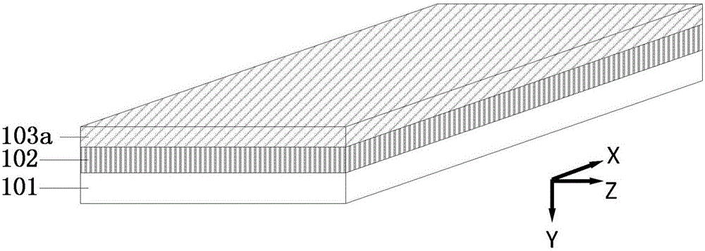
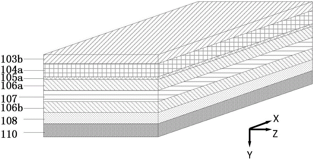
[0077] This embodiment proposes a method for manufacturing a gate-all-around field effect transistor, including the following steps:

[0078] Step 1, forming a bonding metal layer 103, a first gate dielectric layer 105a, a first interface control layer 106a, a channel layer 107, a second interface control layer 106b, a source-drain layer 108 and a semiconductor material layer on the substrate 101 110;

[0079] Step 2, such as Figure 5 As shown, the semiconductor material layer 110 is removed by etching, and as Figure 6 As shown, a convex-shaped structure is formed by etching in the channel region, the protruding part is etched to the second interface control layer 106b, and both sides of the protruding part are etched to the first gate dielectric layer 105a. After etching, the channel region Cross section as Figure 7 shown;

[0080] Step 3, if Figure 8 As shown, a third interface control layer 106c is grown on both side walls of the protruding part of the channel regi...

Embodiment 2

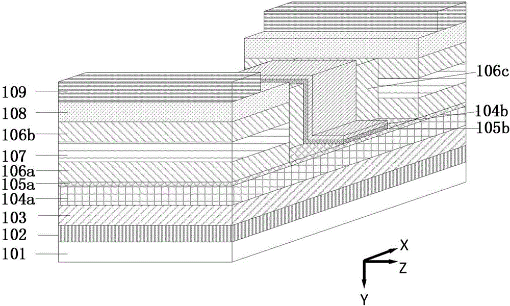
[0103] Such as figure 1 As shown, this embodiment proposes a gate-all-around field effect transistor, which is prepared by the preparation method in Example 1, and includes a source region, a drain region and a channel region, and the channel region is located between the source region and the drain region Between and integral molding, it is characterized in that:

[0104] The longitudinal direction of the channel region is convex; the protruding parts of the source region, the drain region and the channel region are successively stacked with a substrate 101, a first gate dielectric layer 105a, a first interface control layer 106a, a A channel layer 107, a second interface control layer 106b; a substrate 101 and a first gate dielectric layer 105a are sequentially stacked on the platforms on both sides of the protruding part of the channel region;

[0105] The left and right side walls of the protruding part of the channel region have a third interface control layer 106c, and ...


PUM

PropertyMeasurementUnit
thicknessaaaaaaaaaa
thicknessaaaaaaaaaa
thicknessaaaaaaaaaa

Abstract

The invention relates to a ring gate field effect transistor and a preparation method thereof. The preparation method includes the following steps that: a first gate dielectric layer, a channel layer, a second interface control layer, a source-drain layer and a semiconductor material layer are formed on a substrate; the semiconductor material layer is removed through etching, a structure shaped like a Chinese character ''tu' is formed in a channel region along a longitudinal direction through etching, the etching of the protruding part of the structure shaped like a Chinese character ''tu' is performed until arriving at the second interface control layer, and the etching of two sides of the structure shaped like a Chinese character ''tu' is performed until arriving at the first gate dielectric layer; third interface control layers grow on two side walls of the protruding part of the channel region, and a second gate dielectric layer and a second gate metal layer are formed on the upper surface of the protruding part from bottom to top, wherein the upper surface of the protruding part is separated from a source region and a drain region by a certain distance, and the second gate dielectric layer and the second gate metal layer extend to the side walls of the third interface control layers and the upper surfaces of flat stages at two sides of the protruding part; and a source-drain metal layer is formed at a portion at the upper surface of the source-drain layer in the source region and the drain region, wherein the portion is adjacent to the outer side of the upper surface of the source-drain layer. According to the transistor provided by the invention, channel scattering can be decreased, channel carrier mobility, gate control ability and current driving ability can be improved, and a short channel effect and a DIBL effect can be effectively suppressed.

Description

technical field [0001] The invention relates to a semiconductor integrated device, in particular to a ring gate field effect transistor and a preparation method thereof. Background technique [0002] With the proportional reduction of the feature size of devices, the performance of silicon-based CMOS devices and the integration level of integrated circuits have been greatly improved. When CMOS technology enters the 45nm technology node, traditional silicon-based CMOS devices can no longer meet the demand for semiconductor performance. Therefore, the introduction of new materials and new structures has become one of the solutions in the post-Moore era. III-V semiconductor materials Due to its advantages of high electron mobility and wide bandgap width, it has become one of the first choices for channel materials of CMOS devices. At the same time, when the device size enters the 22nm technology node, factors such as short channel effect, source-drain punchthrough and quantum ...

Claims


Application Information

Patent Timeline
Patent Type & Authority Applications(China)
IPC IPC(8): H01L29/10H01L29/20H01L21/336H01L29/78
Inventor 王盛凯李跃刘洪刚马磊孙兵常虎东王博
Owner INST OF MICROELECTRONICS CHINESE ACAD OF SCI
Learn More