

Method for overcoming PETEOS thin film defects and semiconductor structure
A thin-film defect and semiconductor technology, which is applied in semiconductor devices, semiconductor/solid-state device manufacturing, electric solid-state devices, etc., can solve the problems of poor film layer quality and unsatisfactory surface quality of other dielectric films, so as to increase surface activity and reduce Surface hillock defect, effect of reducing hydrogen bond content
- Summary
- Abstract
- Description
- Claims
- Application Information
AI Technical Summary
Problems solved by technology
Method used
Image

Examples
Embodiment 1
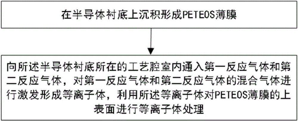
[0031] In step 2 of this embodiment, a mixed gas of oxygen and helium is introduced into the process chamber where the semiconductor substrate is located, the flow rate of oxygen is 4200 sccm, the flow rate of helium is 4000 sccm, the pressure in the process chamber is 5 torr, and the process The radio frequency power of the radio frequency source in the chamber is 790W, and the temperature in the process chamber is 400°C. After the plasma treatment for 5s, the plasma treatment step of step 2 is completed.
Embodiment 2
[0033] In step 2 of this embodiment, a mixed gas of oxygen and argon is introduced into the process chamber where the semiconductor substrate is located, the flow rate of oxygen is 1000 sccm, the flow rate of argon is 1000 sccm, the pressure in the process chamber is 3 torr, and the process The radio frequency power of the radio frequency source in the chamber is 1000W, the temperature in the process chamber is 500°C, and after plasma treatment for 8s, the plasma treatment step of step 2 is completed.
Embodiment 3
[0035] In step 2 of this embodiment, a mixed gas of oxygen and nitrogen is introduced into the process chamber where the semiconductor substrate is located. The flow rate of oxygen is 6000 sccm, the flow rate of nitrogen gas is 5000 sccm, and the pressure in the process chamber is 10 torr. The radio frequency power of the medium radio frequency source is 600W, and the temperature in the process chamber is 300°C. After plasma treatment for 2s, the plasma treatment step of step 2 is completed.
PUM
 Abstract
Description
Claims
Application Information