Chip packaging structure and method

A chip packaging structure and packaging layer technology, which is applied to electrical components, electrical solid devices, circuits, etc., can solve the problems of low chip packaging space utilization and single circuit function

Inactive Publication Date: 2017-05-31
NAT CENT FOR ADVANCED PACKAGING
View PDF6 Cites 5 Cited by
  • Summary
  • Abstract
  • Description
  • Claims
  • Application Information

AI Technical Summary

Problems solved by technology

[0005] The embodiment of the present invention provides a chip packaging structure and method, which can avoid the problems of low util

Method used


Image

  • Chip packaging structure and method
  • Chip packaging structure and method
  • Chip packaging structure and method

Examples


Embodiment 1

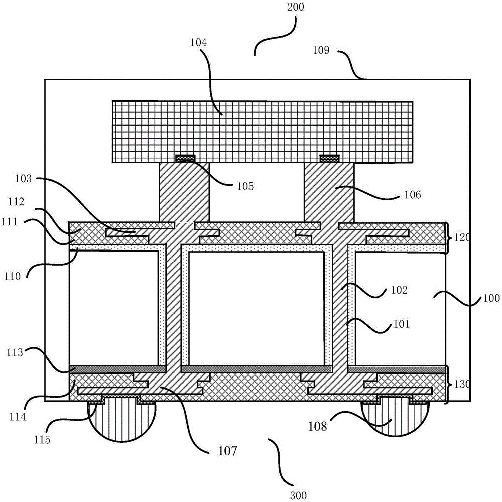
[0041] figure 1 It is a schematic diagram of a chip package structure provided by an embodiment of the present invention. This embodiment is applicable to various chip packaging situations, and is applied to high-end chips, such as Field Programmable Gate Array (Field Programmable Gate Array, FPGA), Graphics Processing Unit (Graphics Processing Unit, GPU), Central Processing Unit (Central Processing Unit , CPU) and high bandwidth memory (High Bandwidth Memory, HBM), etc. A chip packaging structure provided by an embodiment of the present invention includes:

[0042] Base substrate 100, first side 200, second side 300, first redistribution layer 120, second redistribution layer 130, via hole 101, first conductive pillar 102, first redistribution sublayer 103, flip chip 104, electrode 105, second conductive pillar 106, second rewiring sublayer 107, first external connection bump 108, encapsulation layer 109, first insulating layer 110, first passivation layer 112, second diffu...

Embodiment 2

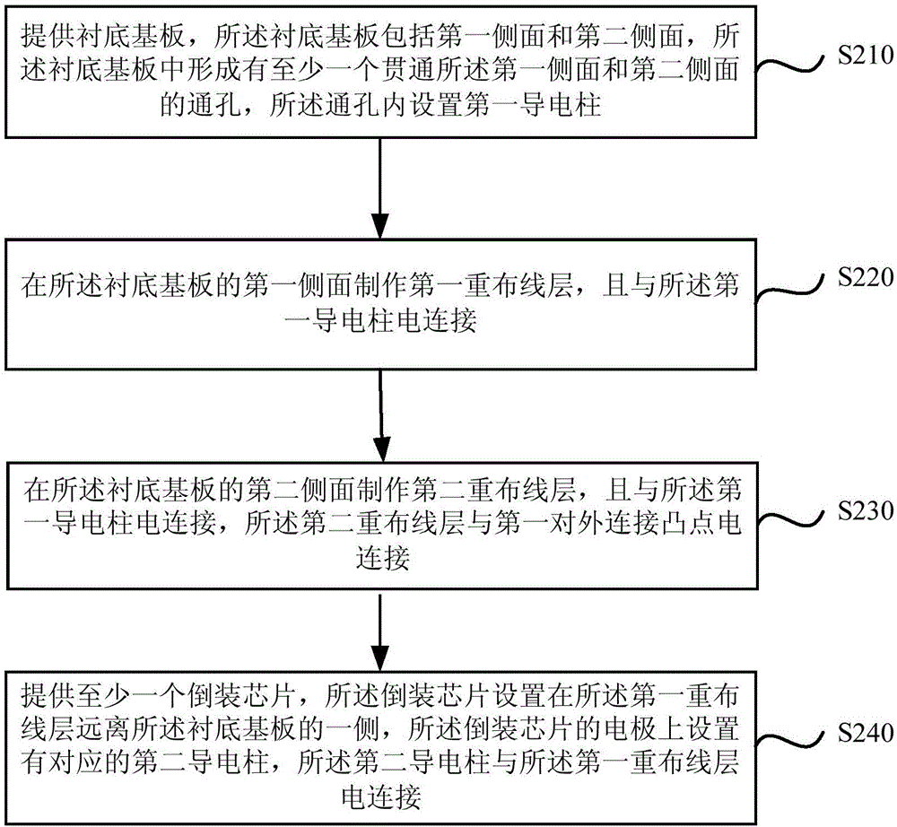
[0056] figure 2 The embodiment of the present invention also provides a flow chart of a chip packaging method, such as figure 2 Shown:

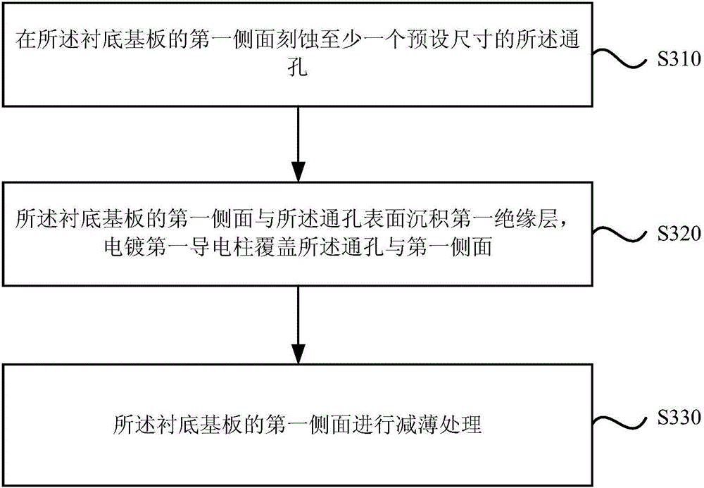
[0057] S210. Provide a base substrate, the base substrate includes a first side and a second side, at least one through hole penetrating through the first side and the second side is formed in the base substrate, and the through hole setting the first conductive column;

[0058] S220. Prepare a first redistribution layer on the first side surface of the base substrate, and electrically connect to the first conductive column;

[0059] S230. Prepare a second redistribution layer on the second side surface of the base substrate, and electrically connect to the first conductive column, and the second redistribution layer is electrically connected to the first external connection bump;

[0060] S240. Provide at least one flip chip, the flip chip is arranged on the side of the first redistribution layer away from the base substrate, and the el...


PUM


Abstract

An embodiment of the invention discloses a chip packaging structure and method. The structure comprises a substrate base board, a first rerouting layer, a second rerouting layer and at least one inverted chip, the substrate base board comprises a first side surface and a second side surface, at least one through hole is formed in the substrate base board and penetrates the first side surface and the second side surface, first conducting posts are arranged in the through holes, the first rerouting layer is arranged on the first side surface of the substrate base board and electrically connected with the first conducting posts, the second rerouting layer is arranged on the second side surface of the substrate base board and electrically connected with the first conducting posts and first external connection projections, the inverted installation chips are arranged on one side of the first rerouting layer far away from the substrate base board, and second corresponding conducting posts are arranged on electrodes of the inverted chips and electrically connected with the first rerouting layer. According to the method, high-integration density of chips is achieved, input/output device interfaces in the unit area of the chips are increased, and electrical properties of the chips are improved.

Description

technical field [0001] The embodiments of the present invention relate to the technical field of chip manufacturing, and in particular to a chip packaging structure and method. Background technique [0002] With the miniaturization and high-performance development of electronic products, the system integration level is also increasing day by day. [0003] Through Silicon Via technology (Through Silicon Via, TSV) technology is a high-density packaging technology, through the filling of conductive substances such as copper, tungsten, polysilicon, etc., to realize the vertical electrical interconnection of through silicon vias. Though-Silicon-Via Interposer (TSV Interposer), as a mainstream branch of 3D SIP technology, mainly adopts a single-layer or multi-layer plug-in stacking form. Fan-out wafer packaging is based on wafer reconfiguration technology, where chips are rearranged on an artificial wafer, and then packaged in steps similar to the standard WLP (Wafer Level Packag...

Claims


Application Information

Patent Timeline
IPC IPC(8): H01L23/31H01L23/488H01L23/498H01L21/60
CPCH01L23/31H01L23/488H01L23/49816H01L24/10H01L24/11
Inventor 王振杰
Owner NAT CENT FOR ADVANCED PACKAGING
Why Eureka
Try Eureka