Field-effect transistor and manufacturing method thereof

A technology for field effect transistors and manufacturing methods, which is applied in semiconductor/solid-state device manufacturing, semiconductor devices, electrical components, etc., and can solve the problems of increasing parasitic parameters of parasitic capacitance and affecting MOSFET performance and reliability, etc.

Active Publication Date: 2017-05-31
HUAWEI TECH CO LTD
View PDF2 Cites 19 Cited by
  • Summary
  • Abstract
  • Description
  • Claims
  • Application Information

AI Technical Summary

Problems solved by technology

[0003] In the above manufacturing method, when the source electrode 14 and the drain electrode 15 are formed by a doping process, as figure 1 As shown, the source 14 (or drain 15) is in direct contact with the first semiconductor material layer 11 and the second semiconductor material layer 12 in the channel 100, so that a part of the impurity atoms diffuse to the second semiconductor materi

Method used


Image

  • Field-effect transistor and manufacturing method thereof
  • Field-effect transistor and manufacturing method thereof
  • Field-effect transistor and manufacturing method thereof

Examples


Embodiment Construction

[0036] The technical solutions in the embodiments of the present invention will be described in detail below in conjunction with the accompanying drawings in the embodiments of the present invention. Obviously, the described embodiments are only some of the embodiments of the present invention, not all of them.

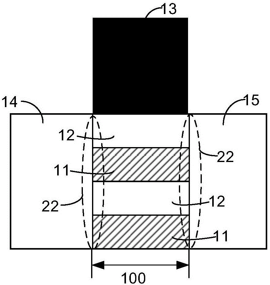
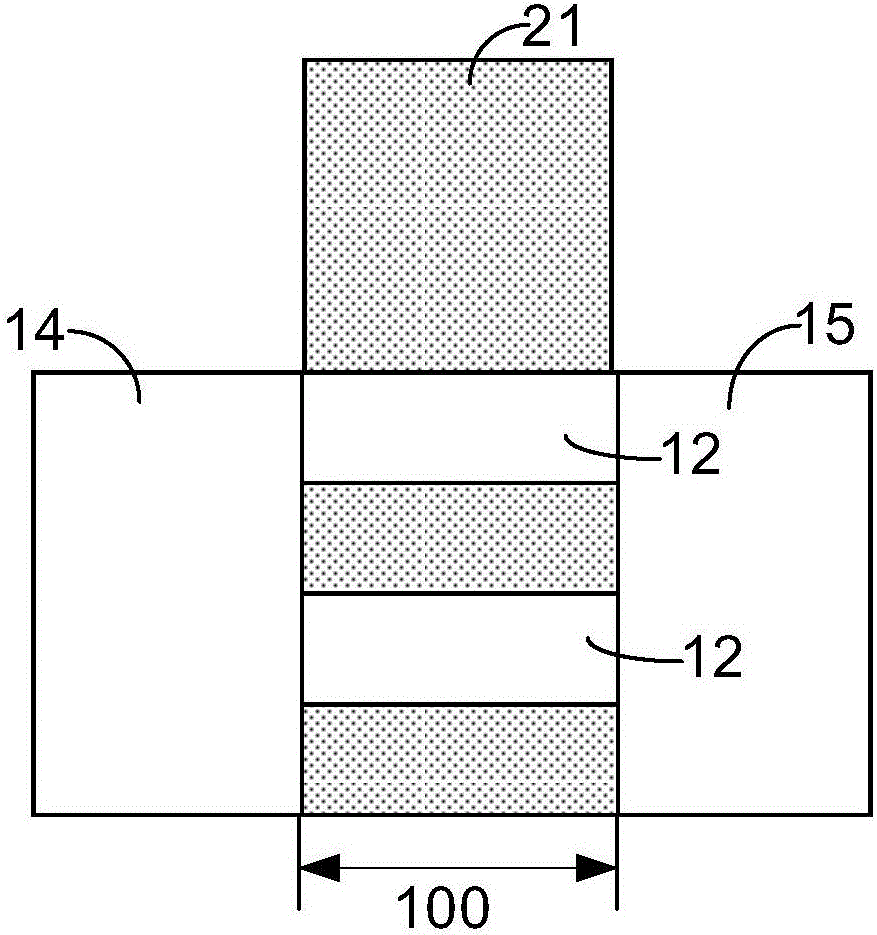
[0037] An embodiment of the present invention provides a field-effect transistor, which can be a MOSFET, for example, a stacked gate-all-around nanowire transistor (Stacked Gate-All-Around Nanowire Transistor), a fin field-effect transistor (Fin Field-Effect Transistor) , FinFET), etc., may also be a tunneling field effect transistor (TFET, Tunneling Field Effect Transistor), etc., which is not limited in this embodiment of the present invention.

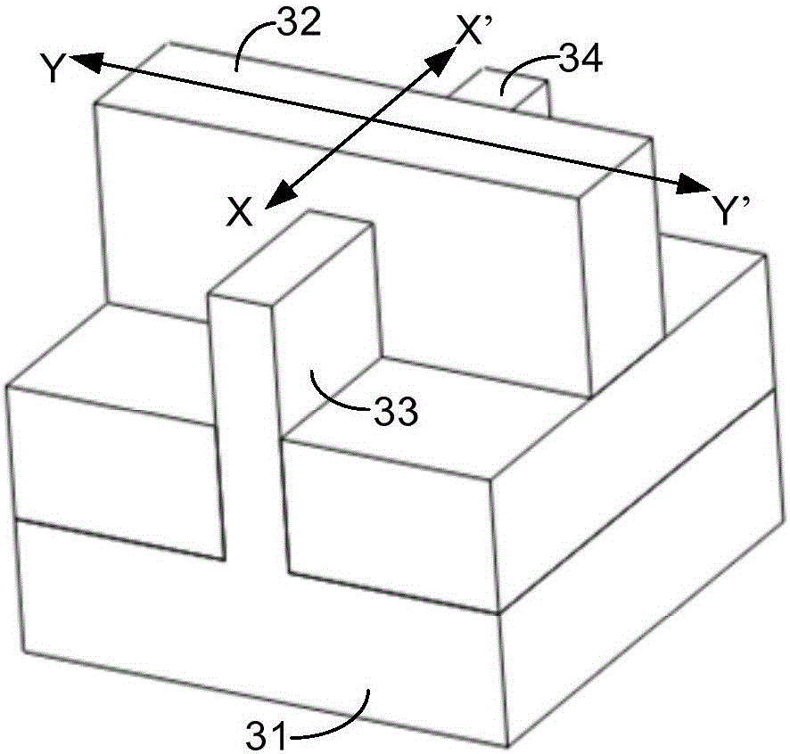
[0038] In addition, in order to provide a field effect transistor and its manufacturing method for the convenience of explaining the embodiments of the present invention, firstly, each cross-sectional direction of the field ...


PUM

PropertyMeasurementUnit
Thicknessaaaaaaaaaa
Thicknessaaaaaaaaaa

Abstract

The embodiment of the invention provides a field-effect transistor and a manufacturing method thereof and relates to the technical field of semiconductors. Parasitic parameters of the field-effect transistor can be reduced to improve the reliability of the field-effect transistor. The method comprises the steps as follows: a support structure with superlattice characteristics is formed on a semiconductor substrate; the support structure comprises first semiconductor material layers and second semiconductor material layers, which are alternately arranged; isolating layers are arranged at two sides of the support structure; a false gate structure covering the support structure is formed along the juncture of the isolating layers and the support structure; the length of the false gate structure in a gate length direction is smaller than those of the first semiconductor material layers in the gate length direction; areas except for sacrificial layers in the first semiconductor material layers are removed along the gate length direction to form insulating grooves; the dielectric constants of mediums filled into the insulating grooves are smaller than those of the first semiconductor material layers; and a source and a drain are formed in preset source region and drain region along the gate length direction and the source and the drain are isolated from the sacrificial layers through the insulating grooves.

Description

technical field [0001] Embodiments of the present invention relate to the technical field of semiconductors, in particular to a field effect transistor and a manufacturing method thereof. Background technique [0002] At present, when making a field-effect transistor (Field-Effect Transistor, FET), take a MOSFET (Metal-Oxide-Semiconductor Field-Effect Transistor, Metal-Oxide Semiconductor Field-Effect Transistor) as an example, such as figure 1 As shown, the first semiconductor material layer 11 and the second semiconductor material layer 12 are generally stacked in sequence in the channel 100, as well as the dummy gate structure 13 located on the second semiconductor material layer 12, and the source and drain regions on both sides of the channel 100 After the source electrode 14 and the drain electrode 15 are formed by the doping process, the second semiconductor material layer 12 and the dummy gate structure 13 can be removed by an etching process, and then, as figure 2...

Claims


Application Information

Patent Timeline
IPC IPC(8): H01L29/78H01L21/336
CPCH01L29/66545H01L29/66787H01L29/78H01L29/785B82Y10/00H01L29/0673H01L29/42392H01L29/7613H01L29/66469H01L29/0653H01L29/78696H01L29/66742H01L29/78684H01L29/775
Inventor 马小龙张日清斯蒂芬.巴德尔
Owner HUAWEI TECH CO LTD
Why Eureka
Try Eureka