Variable coding method for implementing chip reuse and communication terminal thereof

一种编码方法、芯片的技术,应用在可变编码,通信终端领域,能够解决适用范围有限、抗干扰问题难以解决等问题,达到降低开发成本、简化芯片种类的效果

Active Publication Date: 2017-06-06
VANCHIP TIANJIN TECH
View PDF4 Cites 1 Cited by
  • Summary
  • Abstract
  • Description
  • Claims
  • Application Information

AI Technical Summary

Problems solved by technology

However, the existing component reusable technology still has many defects such as limited scope of application and difficulty in solving anti-interference problems.

Method used


Image

  • Variable coding method for implementing chip reuse and communication terminal thereof
  • Variable coding method for implementing chip reuse and communication terminal thereof
  • Variable coding method for implementing chip reuse and communication terminal thereof

Examples


Embodiment 1

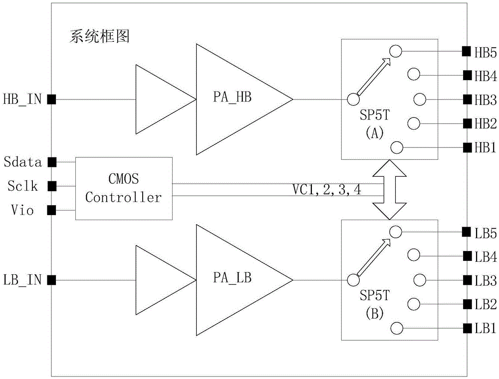
[0039] figure 1 It is a system block diagram of a radio frequency power amplifier (PA) and a radio frequency switch module used in a communication terminal. Among them, the RF front-end uses two single-pole five-throw (SP5T) RF switch chips, their working principle is the same, and the source (CMOS Controller) of the logic input signals VC1-VC4 used to control them is also the same. However, since the integrated circuit system requires these two RF switch chips to undertake the work of switching RF signals in different frequency bands (such as high frequency band and low frequency band), they are irreplaceable from the system level and must coexist. Circuit chips, but the only difference between them is the truth table of their control logic.

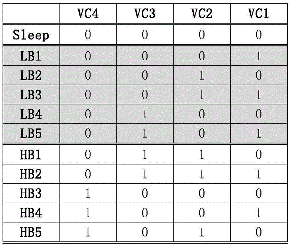
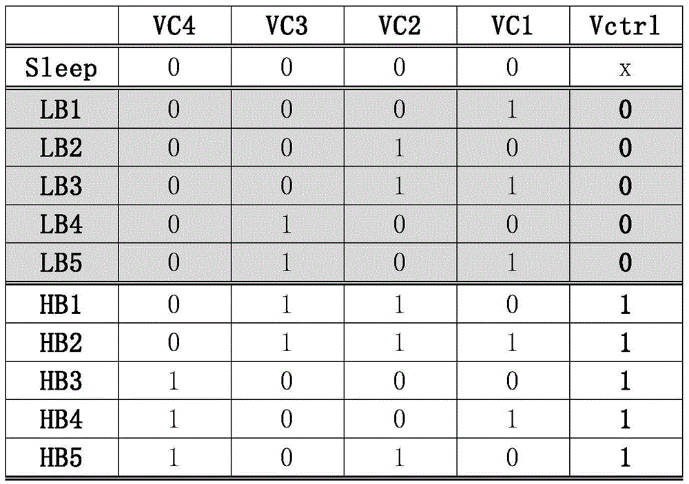
[0040] Such as figure 2 As shown, the control logic truth tables defined by the integrated circuit system for the high frequency band (HB) and the low frequency band (LB) are different. In order to realize these functions, two diffe...

Embodiment 2

[0048] Such as Figure 7 As shown, in another embodiment of the present invention, in the circuit design stage, the input terminal of the logic control signal Vctrl is pulled up to the power supply (VDD) terminal through a slightly larger resistor, and then applied to the high frequency band (HB) radio frequency The Vctrl pin of the RF switch chip A of the signal can be suspended (it does not need to be connected to a fixed level in the packaging stage), at this time, only the Vctrl pin of the RF switch chip B needs to be connected to the ground (GND) terminal, thereby reducing A wire (Wire Bonding) to the power supply (VDD) terminal.

[0049] The pull-up resistors mentioned here are not limited to passive thin-film resistors, and may also be various types of transistors with appropriate bias states. The selection of its resistance value or equivalent resistance needs to be considered in a compromise: it is necessary to consider the strength of the pull-up to resist interfere...

Embodiment 3

[0051] Such as Figure 8 As shown, in another embodiment of the present invention, the input terminal of the logic control signal Vctrl is pulled down to the ground (GND) end through a slightly larger resistor, and then the radio frequency switch chip applied to the low frequency band (LB) radio frequency signal The Vctrl pin of B can be suspended (it does not need to be connected to a fixed level in the packaging stage), at this time, only the Vctrl pin of the RF switch chip A needs to be connected to the power supply (VDD) terminal, thus reducing the one to the ground ( GND) end of the wire (Wire Bonding).

[0052] The pull-down resistors mentioned here are not limited to passive thin-film resistors, and may also be various types of transistors with appropriate bias states. The selection of its resistance value or equivalent resistance value needs to be considered in a compromise: it is necessary to consider the strength of the pull-down to resist interference, which requir...


PUM


Abstract

The invention discloses a variable coding method for implementing chip reuse. The method includes the following steps: using at least two same integrated circuit chips of which each controls logic truth tables based on the differences of gating signals; introducing at least one logical control signal as a gating signal; controlling the logic control signal, such that respective integrated circuit chip controls the logic truth table accordingly. The invention also discloses a communication terminal for implementing chip reuse by using the variable coding method. According to the invention, two completely identical integrated circuit chips or more are enabled to implement different logic control, so that chip types that implement system functions are reduced, development cost of an integrated circuit system is greatly reduced as well as supply chains for mass production.

Description

technical field [0001] The invention relates to a variable coding method for realizing chip reuse, and also relates to a communication terminal using the variable coding method for realizing chip reuse, belonging to the technical field of integrated circuits. Background technique [0002] The pursuit of miniaturization, multi-function, low cost and low power consumption of electronic products is endless, which makes process improvement and system integration the two major development trends of the semiconductor industry. At present, the wafer manufacturing industry, which emphasizes process improvement, is still developing in accordance with Moore's Law. However, with the further shrinking of process dimensions, Moore's Law is gradually going to the limit. [0003] System integration is an important technical approach for the semiconductor industry to surpass Moore's Law. Currently, there are three mainstream technologies for system integration: System in Package (SiP for ...

Claims


Application Information

Patent Timeline
Patent Type & Authority Applications(China)
IPC IPC(8): H03K19/00
CPCH03K19/0002H03K19/00307H03K19/08H03K19/212H04B14/00
Inventor 林升
Owner VANCHIP TIANJIN TECH
Why Eureka
Try Eureka