Manufacturing method of flexible substrate and flexible display panel
A technology of flexible display and manufacturing method, which is applied in nonlinear optics, identification devices, instruments, etc., to achieve the effect of reducing the height of protrusions
- Summary
- Abstract
- Description
- Claims
- Application Information
AI Technical Summary
Problems solved by technology
Method used
Image
Examples
Embodiment 1
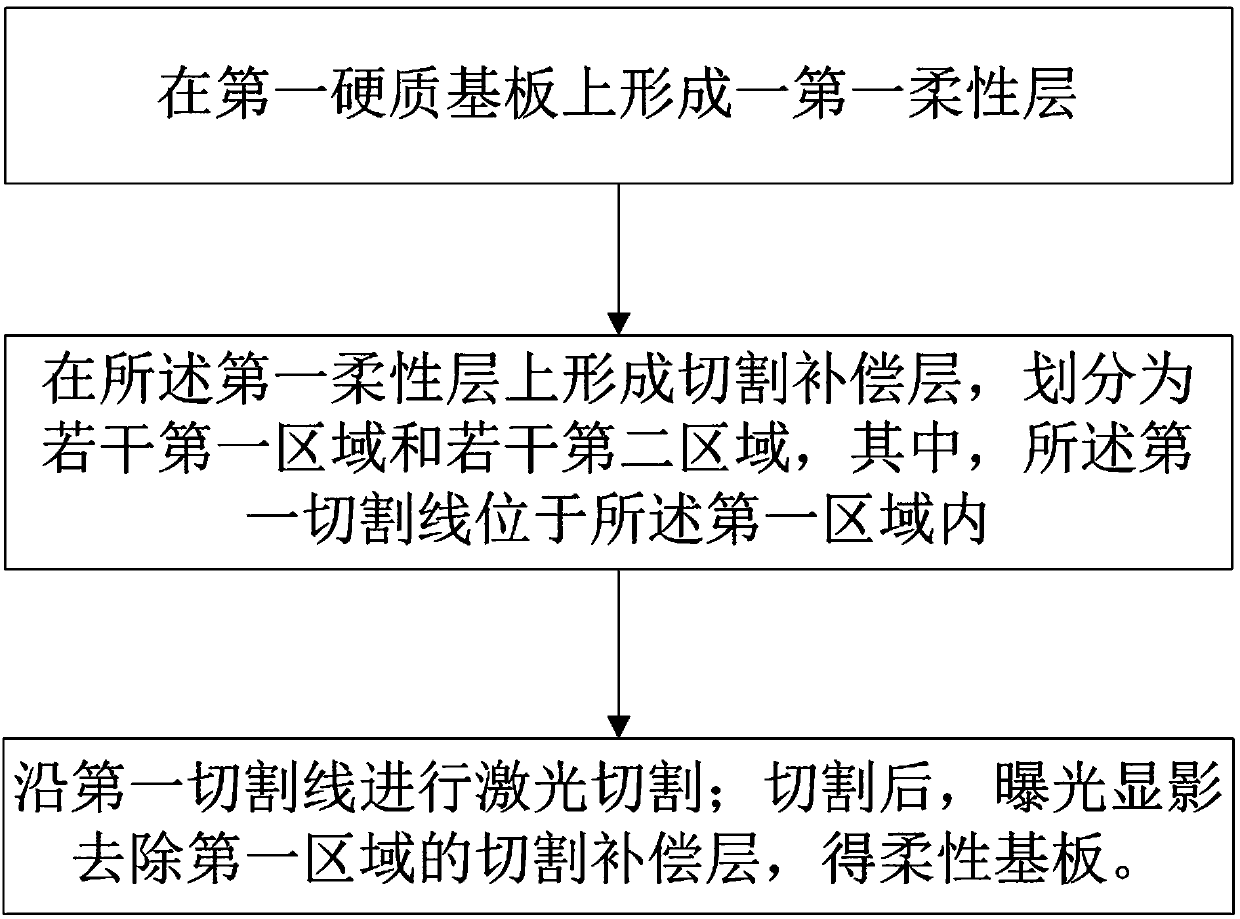
[0042] In order to solve the above problems, the present invention provides a method for manufacturing a flexible substrate, which includes the following steps:
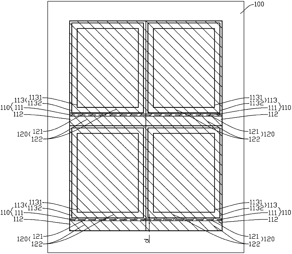
[0043] Step A1, forming a first flexible layer 100 on the first hard substrate.
[0044] The first flexible layer 100 is divided into several first panel areas 110, each of which includes a cutting area 112 and a non-cutting area 113 separated by a first cutting line 111; the non-cutting area 113 It includes a first display area 1131 and a first sealing area 1132 surrounding the first display area 1131 .
[0045] The material of the hard substrate is preferably but not limited to glass, such as alkali-free glass. The material of the flexible layer includes organic polymer materials, preferably but not limited to PI, TAC; the usual thickness is about 50-100 μm. In order to realize the separation of flexible structures, it is often necessary to use a glass substrate as a support for the flexible substrate. The glass...
Embodiment 2
[0054] The present invention also provides a method for manufacturing a flexible display panel, which includes the following steps:
[0055] Step B1, providing the flexible substrate of Example 1.
[0056] Step B2, forming a color filter assembly on each non-cutting area 113 of the flexible substrate in step B1 to obtain a flexible color filter substrate.
[0057] Each of the non-cutting areas 113 includes a first display area 1131 and a first sealing area 1132 surrounding the first display area 1131 . Forming the color filter assembly on the non-cutting area 113 specifically includes the following steps:
[0058] In the non-cutting area 113, a black matrix is formed on the first flexible layer on which the cutting compensation layer has been formed;
[0059] In the first display area 1131 , a color filter layer is formed on the first flexible layer on which the black matrix has been formed.
[0060] Preferably, it also includes:
[0061] In the non-cutting area 113, a t...
Embodiment 3
[0075] The present invention also provides a method for manufacturing a flexible display panel, which includes the following steps:
[0076] Step C1, providing the flexible substrate of Example 1;
[0077] Step C2, forming a display device in the first display area 1131 on each non-cutting area 113 of the flexible substrate in step C1, to obtain a flexible array substrate.
[0078] It should be noted that the display device includes an electronic component layer and a display material layer; wherein the electronic component layer includes thin film transistors, electrophoretic display components, organic light emitting diode display components, scanning lines, data lines, display electrodes, etc., The production process is such as coating, deposition, etching, high temperature treatment, etc.; the display material layer can be various films with realistic characteristics such as liquid crystal layer, organic light-emitting layer, electrochromic layer, electronic ink layer, cho...
PUM
| Property | Measurement | Unit |
|---|---|---|
| thickness | aaaaa | aaaaa |
| width | aaaaa | aaaaa |
| thickness | aaaaa | aaaaa |
Abstract
Description
Claims
Application Information


