Silica-based three-dimensional heterogeneously-integrated radio frequency microsystem and manufacturing method thereof

A micro-system and radio-frequency technology, which is applied in the manufacture of micro-structure devices, micro-structure technology, micro-structure devices, etc., can solve the problems of interconnection occupation area, signal transmission length and delay increase, and difficult to meet, so as to reduce the size, Good performance consistency, performance-enhancing effects

Pending Publication Date: 2018-05-29
GREAT MICROWAVE TECH CO LTD
View PDF6 Cites 33 Cited by
  • Summary
  • Abstract
  • Description
  • Claims
  • Application Information

AI Technical Summary

Problems solved by technology

Since MCM can only achieve three-dimensional high-density interconnection through the substrate, the characteristic size of the interconnection lines can only be tens of microns to hundreds of microns due to process constraints, and the chips are arranged in a horizontal manner. The occupied area, signal transmission length and delay will increase rapidly with the increase of the number of chips and I / O pins, and it is difficult to meet the needs of future RF microsystems / electronic modules in high density, high-speed interconnection, compact appearance, Technical requirements for various types of devices

Method used


Image

  • Silica-based three-dimensional heterogeneously-integrated radio frequency microsystem and manufacturing method thereof
  • Silica-based three-dimensional heterogeneously-integrated radio frequency microsystem and manufacturing method thereof
  • Silica-based three-dimensional heterogeneously-integrated radio frequency microsystem and manufacturing method thereof

Examples


Embodiment Construction

[0032] The present invention will be further described below in conjunction with the accompanying drawings and embodiments.

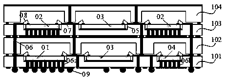
[0033] as attached figure 1 As shown, it is a schematic structural diagram of a silicon-based three-dimensional heterogeneous integrated radio frequency microsystem of the present invention, including a first silicon substrate layer 101, a second silicon substrate layer 102, a third silicon substrate layer 103, a fourth silicon substrate layer 104, RF power amplifier chip 01, RF low noise amplifier chip 02, RF filter 03 and RF switch 04; the front of the first silicon substrate layer 101 and the third silicon substrate layer 103, the second silicon substrate layer 102 and the fourth silicon substrate layer 104 The back side of each is provided with an etched cavity 05; the first silicon substrate layer 101, the second silicon substrate layer 102, the third silicon substrate layer 103 and the fourth silicon substrate layer 104 are all provided with throu...


PUM

PropertyMeasurementUnit
electrical resistivityaaaaaaaaaa

Abstract

The invention discloses a silica-based three-dimensional heterogeneously-integrated radio frequency microsystem and a manufacturing method thereof. The silica-based three-dimensional heterogeneously-integrated radio frequency microsystem comprises a first silica substrate layer, a second silica substrate layer, a third silica substrate layer, a fourth silica substrate layer, a radio frequency power amplification chip, a radio frequency low noise amplification chip, a radio frequency filter and a radio frequency switch, wherein the silica substrate layers are high-resistance silicon wafers; radio frequency chips and devices are made of different substrate materials through different processes; the radio frequency chips and devices are assembled inside cavities pre-etched in the first silicasubstrate layer and the third silica substrate layer; the first silica substrate layer, the second silica substrate layer, the third silica substrate layer and the fourth silica substrate layer are processed through low-temperature wafer-scale bonding into a whole and vertically connected through silicon through holes to form the silica-based three-dimensional heterogeneously-integrated radio frequency microsystem. The silica-based three-dimensional heterogeneously-integrated radio frequency microsystem achieves tree-dimensional integration of heterogeneous radio frequency chips and devices,thereby reducing the size, increasing the packaging density, reducing transmission loss of wire connection and enhancing the properties.

Description

technical field [0001] The invention belongs to the technical field of semiconductors, and in particular relates to a silicon-based three-dimensional heterogeneously integrated radio frequency microsystem and a manufacturing method thereof. Background technique [0002] At present, the traditional multi-chip module packaging technology (Multi Chip Module, MCM) is a representative technology in high-density electronic packaging technology. It can easily realize the integration of active / passive circuits, baseband / RF circuits, and is widely used in electronic systems. application. Since MCM can only achieve three-dimensional high-density interconnection through the substrate, the characteristic size of the interconnection lines can only be tens of microns to hundreds of microns due to process constraints, and the chips are arranged in a horizontal manner. The occupied area, signal transmission length and delay will increase rapidly with the increase of the number of chips and...

Claims


Application Information

Patent Timeline
Patent Type & Authority Applications(China)
IPC IPC(8): B81B7/00B81C1/00
CPCB81B7/0032B81C1/00349
Inventor 陈雪平王志宇张勋朱丹丹田锋
Owner GREAT MICROWAVE TECH CO LTD
Why Eureka
Try Eureka