Flexible stretchable conductive circuit and preparation method and use thereof
A conductive line, flexible technology, applied in the direction of printed circuit manufacturing, printed circuit, conductive pattern formation, etc., can solve the problems that are not suitable for fine pattern preparation and large-scale production, affect electrical performance, and pattern structure
- Summary
- Abstract
- Description
- Claims
- Application Information
AI Technical Summary
Problems solved by technology
Method used
Image
Examples
Embodiment 1
[0095] This example is used to illustrate the flexible and stretchable conductive circuit prepared by the method of the present invention.
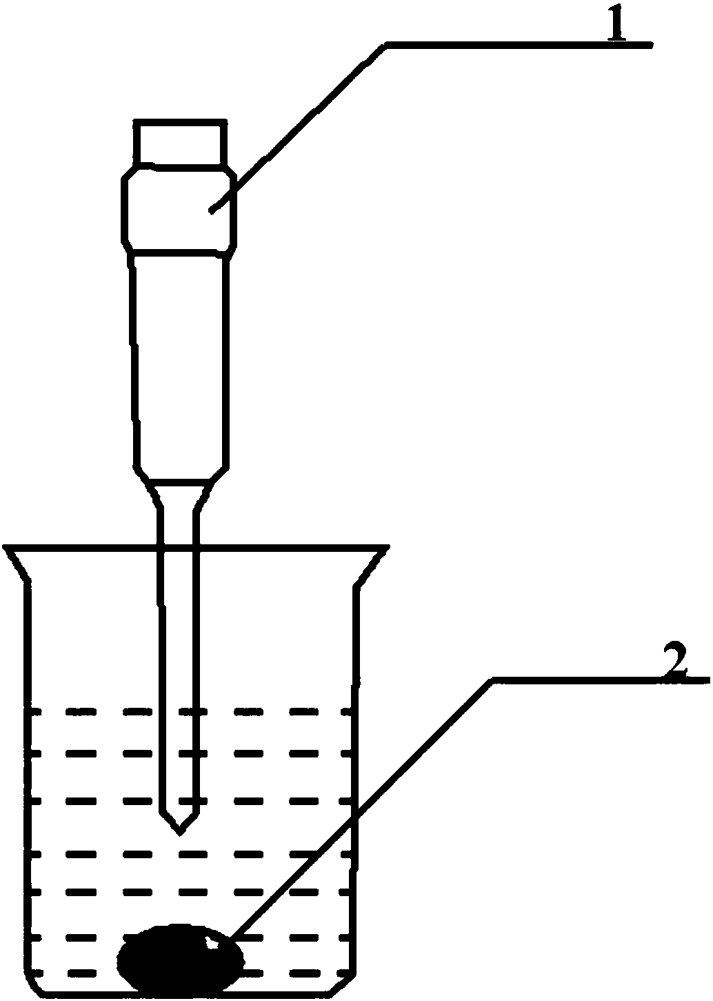
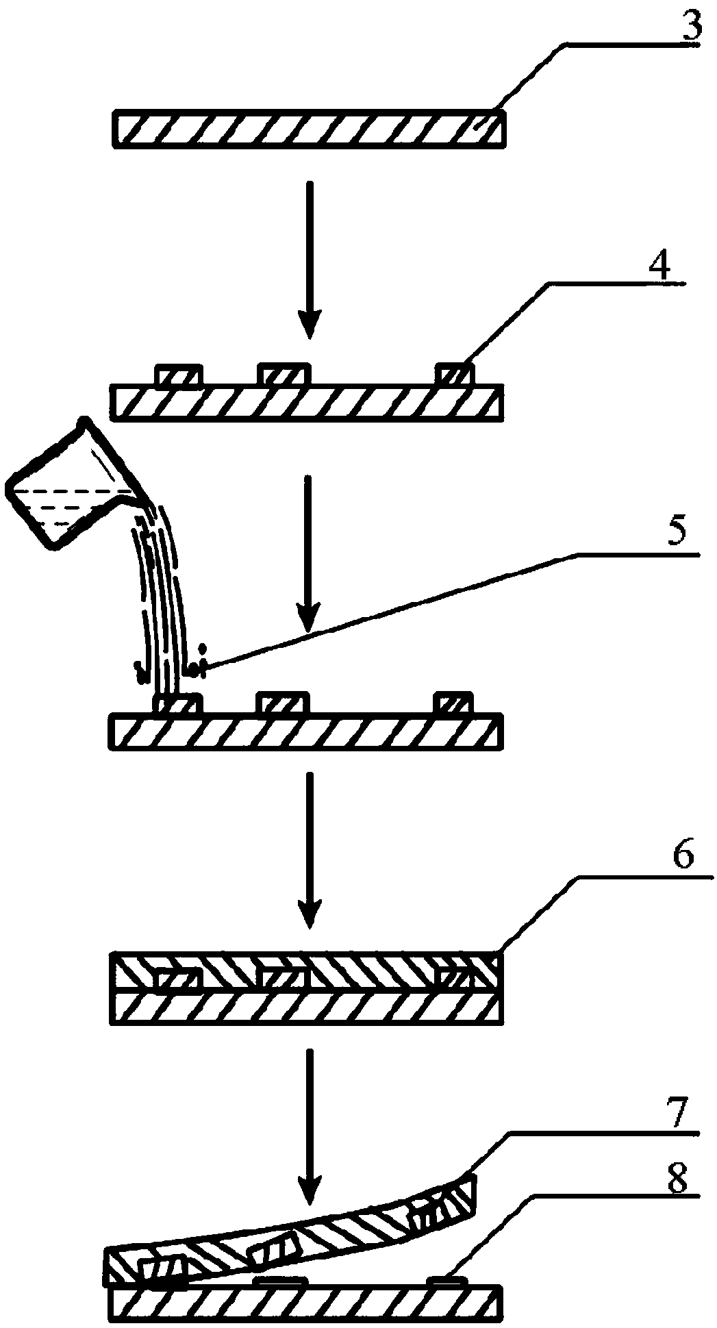
[0096] Put 1g of liquid indium gallium eutectic alloy (EGaIn Ga 75.5%wt In 24.5%wt) in 1ml of mixed solution of n-octanol and glycerol (volume ratio octanol: glycerol=80:20), use Ultrasonic cell disruptor ultrasonicated at 30% amplitude for 60s to obtain a gray liquid metal suspension. The metal was dispersed into numerous micro-nano sized particles with an average particle size of 1500nm. The core of the small particles is liquid metal, and the outside is covered by a thin oxide film. In order to achieve complete transfer, the PET film was selected as the original pattern layer, and the PDMS solution was prepared according to the ratio of PDMS prepolymer: curing agent mass ratio of 10:1. Line widths of 200, 300, 500, 600, 800 and 1000 microns were produced on PET films using screen printing techniques, such as Figure 9 , and its width...
Embodiment 2
[0098] This example is used to illustrate the flexible and stretchable conductive circuit prepared by the method of the present invention. Put 1 g of liquid indium-gallium-tin alloy (In(22)Ga(68)Sn(10)) in 1 ml of 1,4-butyrolactone, and use an ultrasonic cell disruptor to sonicate at 30% amplitude for 30 minutes to obtain the average Ink with a particle size of 600nm. The present invention uses soft etching technology to prepare microfluidic channels with a depth of 80 microns and a width of 200 microns, 100 microns, 80 microns, 50 microns and 20 microns on the surface of the elastomer PDMS, and then fills the ink into the groove with a scraper A pattern is formed in the channel, that is, the PDMS layer is the original pattern layer. Place the pattern in an oven at 80 degrees Celsius for 30 minutes. Then use Smooth-On Ecoflex 0030 as a release layer to cast over the pattern. After being cured at room temperature for 6 hours and peeled off from the PDMS, conductive patterns ...
Embodiment 3
[0100] This example is used to illustrate the flexible and stretchable conductive circuit prepared by the method of the present invention.
[0101] Put 1g of liquid indium-gallium-tin alloy (In(22)Ga(68)Sn(10)) in 1ml of N-methylpyrrolidone, and use an ultrasonic cell disruptor to sonicate at 30% amplitude for 30min to obtain the average particle size 600nm ink. In order to achieve complete transfer, the PET film was selected as the original pattern layer, and the PDMS solution was prepared according to the ratio of PDMS prepolymer: curing agent mass ratio of 10:1. Use inkjet printing method to print the desired pattern on the PET film. That is to say, the prepared ink is added to a piezoelectric nozzle or a thermal bubble nozzle, and the diameter of the nozzle is 40-200 microns. The nozzle prints the required pattern in the preset trajectory. Other steps are as shown in Example 1. We can obtain conductive patterns by inkjet printing.
PUM
 Abstract
Description
Claims
Application Information


