Semiconductor device and manufacturing method thereof, and electronic device

A manufacturing method and semiconductor technology, applied in semiconductor/solid-state device manufacturing, semiconductor devices, electric solid-state devices, etc., can solve problems such as chip damage, affecting device yield and performance, and achieve damage prevention, improve yield and performance, The effect of simple and easy manufacturing method

Active Publication Date: 2017-06-30
SEMICON MFG INT (SHANGHAI) CORP +1
View PDF6 Cites 2 Cited by
  • Summary
  • Abstract
  • Description
  • Claims
  • Application Information

AI Technical Summary

Problems solved by technology

However, due to the thinning of the substrate, it is easy to break the chip during subsequent dicing, which affects the yield and performance of the device

Method used


Image

  • Semiconductor device and manufacturing method thereof, and electronic device
  • Semiconductor device and manufacturing method thereof, and electronic device
  • Semiconductor device and manufacturing method thereof, and electronic device

Examples


Embodiment 1

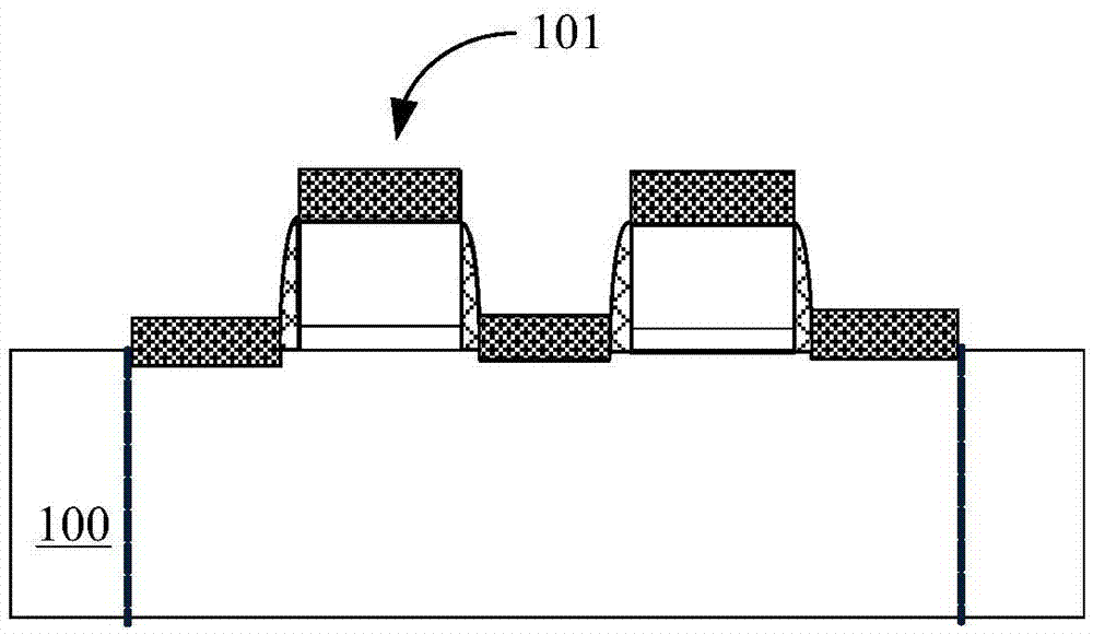
[0046] Below, refer to Figure 1A to Figure 1G as well as figure 2A method for manufacturing a semiconductor device proposed by an embodiment of the present invention will be described. Exemplarily, the semiconductor device of the present invention is a backside illuminated (BSI) image sensor, wherein, Figures 1A-1G It shows a schematic diagram of the device obtained in the relevant steps of the manufacturing method of the semiconductor device in an embodiment of the present invention, figure 2 A schematic flowchart of a method for manufacturing a semiconductor device according to an embodiment of the present invention is shown.

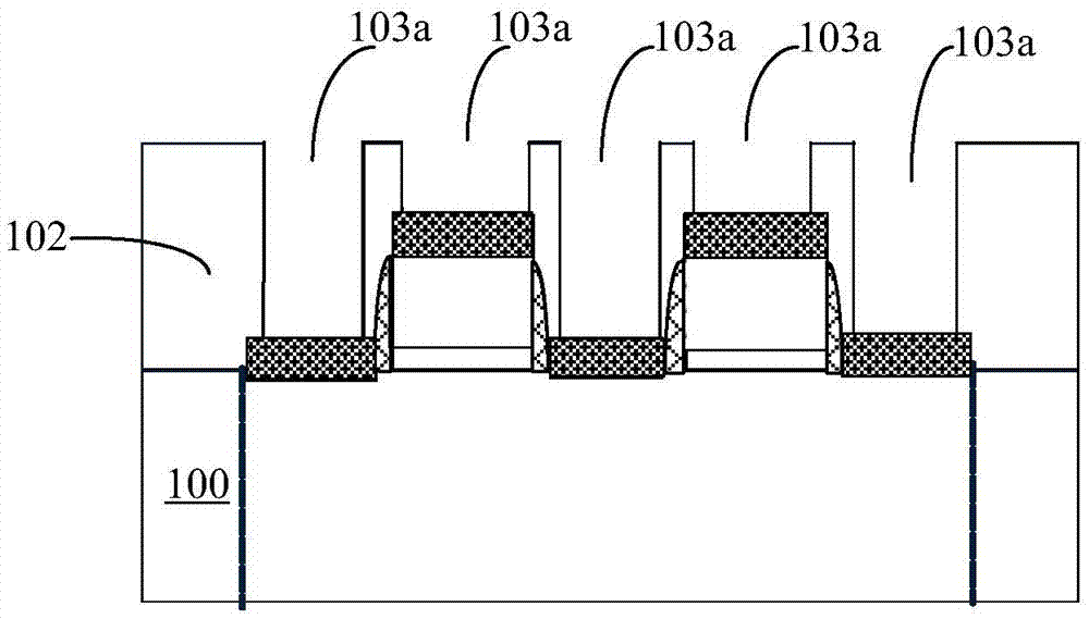
[0047] First, if Figure 1A As shown, a device substrate 100 is provided, and a front-end device 101 is formed on the front side of the device substrate 100 .

[0048] Specifically, the device substrate 100, the device substrate 100 may be at least one of the materials mentioned below: silicon, silicon-on-insulator (SOI), silicon-on-insulator (...

Embodiment 2

[0081] Below, refer to Figure 1G The semiconductor device proposed by the embodiment of the present invention will be described. Exemplarily, the semiconductor device of the present invention is a backside illuminated (BSI) image sensor.

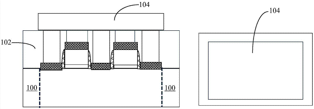
[0082] Such as Figure 1G As shown, the semiconductor device of the present invention includes: a device substrate 100, a front-end device 101 formed on the front side of the device substrate 100, an interlayer dielectric layer 102 covering the front-end device 1011, and a front-end device 101 located on the front-end device 101 The sealing ring 105 that penetrates the interlayer dielectric layer 102 and is partly located in the device substrate 100 in other regions.

[0083] Specifically, the device substrate 100, the device substrate 100 may be at least one of the materials mentioned below: silicon, silicon-on-insulator (SOI), silicon-on-insulator (SSOI), and germanium-on-insulator Silicon (S-SiGeOI), silicon germanium on insulator (Si...

Embodiment 3

[0095] The present invention also provides an electronic device, which includes the semiconductor device in the aforementioned second embodiment, or it includes the semiconductor device formed by the manufacturing method in the aforementioned first embodiment.

[0096] The electronic device of this embodiment can be any electronic product or equipment such as mobile phone, tablet computer, notebook computer, netbook, game console, TV set, VCD, DVD, navigator, camera, video recorder, voice recorder, MP3, MP4, PSP, etc. , can also be any intermediate product including the aforementioned semiconductor device. Due to the use of the above-mentioned semiconductor device, the semiconductor device has excellent performance, so the electronic device of the embodiment of the present invention also has better performance.


PUM


Abstract

The invention provides a semiconductor device and a manufacturing method thereof, and an electronic device, and relates to the technical field of semiconductors. The manufacturing method comprises a device substrate and forming a front-end device on the front side of the device substrate; forming an interlayer dielectric layer through deposition to cover the front-end device and the front side of the exposed device substrate; forming a patterned mask layer on the interlayer dielectric layer in order to cover an area corresponding to the front-end device and make the area except the front-end device be exposed; etching the interlayer dielectric layer in the exposed area except the front-end device and part of the device substrate sequentially by taking the patterned mask layer as the mask to form a sealing ring opening; removing the patterned mask layer; and forming a metal layer through deposition to fill the sealing ring opening in order to form a sealing ring arranged in the area except the front-end device. According to the manufacturing method, the sealing ring is formed in a way of surrounding the front-end device, and is helpful for releasing the stress during the subsequent cutting process, damage to the chip can be prevented, and the yield rate and the performance of the semiconductor device are increased.

Description

technical field [0001] The present invention relates to the technical field of semiconductors, in particular to a semiconductor device, a manufacturing method thereof, and an electronic device. Background technique [0002] Compared with the front-illuminated (FSI) image sensor, the back-illuminated (BSI) image sensor can reduce / avoid the absorption and reflection of light by the circuit layer or oxide layer, so it has higher sensitivity and signal-to-noise ratio. [0003] In the existing BSI process, it is often necessary to perform a back grinding process on the device substrate, and the thickness of the device substrate after grinding is about 3-4 μm. However, due to the thinning of the substrate, it is easy to break the chip during subsequent dicing, which affects the yield and performance of the device. [0004] Therefore, it is necessary to propose a new semiconductor device and its manufacturing method to solve the above technical problems. Contents of the inventio...

Claims


Application Information

Patent Timeline
Patent Type & Authority Applications(China)
IPC IPC(8): H01L27/146H01L21/78
CPCH01L27/1464H01L27/14683H01L21/78
Inventor 李凤莲倪景华
Owner SEMICON MFG INT (SHANGHAI) CORP
Why Eureka
Try Eureka