Gallium-nitride-based inverter chip and forming method therefor

A gallium nitride based, inverter technology, applied in semiconductor devices, semiconductor/solid-state device manufacturing, electrical components, etc., can solve the problems of low operating frequency, poor transmission, low frequency band, etc. On-resistance, effect of wide operating frequency

Active Publication Date: 2017-06-30
SHANGHAI SIMGUI TECH
View PDF4 Cites 2 Cited by
  • Summary
  • Abstract
  • Description
  • Claims
  • Application Information

AI Technical Summary

Problems solved by technology

However, there are generally disadvantages such as complex circuits, low integration, low power, low operating frequency, low frequency band, poor transmission, and weak load capacity. It is necessary to form an inverter with higher performance.

Method used


Image

  • Gallium-nitride-based inverter chip and forming method therefor
  • Gallium-nitride-based inverter chip and forming method therefor
  • Gallium-nitride-based inverter chip and forming method therefor

Examples


Embodiment Construction

[0020] The specific implementation of the gallium nitride-based inverter chip and its forming method provided by the present invention will be described in detail below with reference to the accompanying drawings.

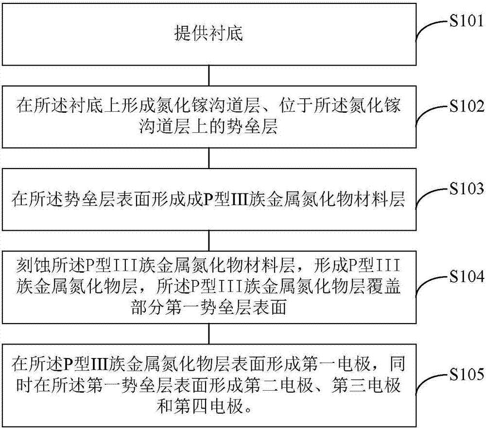
[0021] Please refer to figure 1 , is a schematic flowchart of a method for forming a GaN-based inverter chip according to a specific embodiment of the present invention.

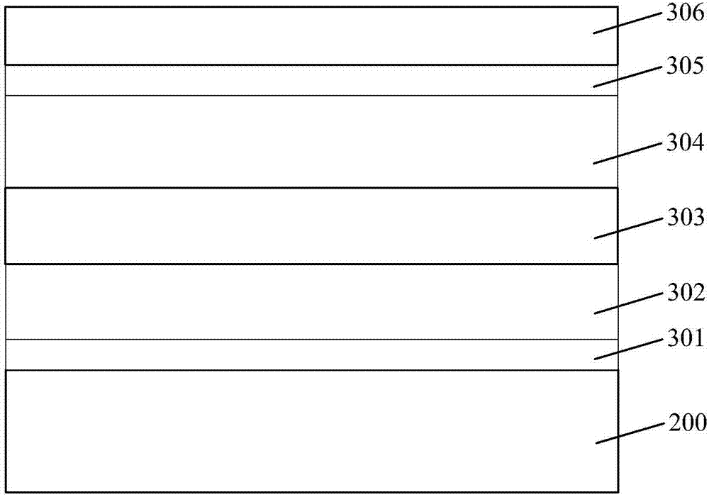
[0022] The method for forming the gallium nitride-based inverter chip includes: step S101: providing a substrate; step S102: forming a gallium nitride channel layer on the substrate, and forming a gallium nitride channel layer on the gallium nitride channel layer Barrier layer; step S103: forming a p-type group III metal nitride material layer on the surface of the barrier layer; step S104: etching the p-type group III metal nitride material layer to form a p-type group III metal nitride material layer layer, the P-type Group III metal nitride layer covers part of the surface of the barrier laye...


PUM

PropertyMeasurementUnit
thicknessaaaaaaaaaa
electrical resistivityaaaaaaaaaa
thicknessaaaaaaaaaa

Abstract

The invention discloses a gallium-nitride-based inverter chip and a forming method therefor, and the chip comprises a substrate; a gallium nitride channel layer located on the substrate; a barrier layer located on the gallium nitride channel layer; a P-type III-family metal nitride layer located on the surface of the barrier layer; a first electrode located on the surface of the P-type III-family metal nitride layer; a second electrode, a third electrode and a fourth electrode, which are all located on the surface of the barrier layer. The chip is good in transmission performance, and is strong in loading capability.

Description

technical field [0001] The invention relates to the technical field of semiconductors, in particular to a gallium nitride-based inverter chip and a forming method thereof. Background technique [0002] Gallium nitride (GaN), as a representative of the third-generation semiconductor materials, has the characteristics of large band gap, high electron drift speed, high thermal conductivity, high voltage resistance, thermal decomposition resistance, corrosion resistance and radiation resistance. [0003] Since the forbidden band width of AlGaN in the AlGaN / GaN heterostructure is larger than that of GaN, at the intersecting interface, a potential barrier is formed on the AlGaN side, and a quasi-triangular potential well is formed on the GaN side, so that the electrons at the interface are in the horizontal direction It can move freely, but is confined in the quasi-triangular potential well in the direction perpendicular to the interface, which is called two-dimensional electron g...

Claims


Application Information

Patent Timeline
Patent Type & Authority Applications(China)
IPC IPC(8): H01L29/778H01L29/423H01L29/47H01L29/20H01L21/335
CPCH01L29/2003H01L29/42316H01L29/475H01L29/66462H01L29/778
Inventor 刘春雪闫发旺张峰赵倍吉李晨
Owner SHANGHAI SIMGUI TECH
Why Eureka
Try Eureka