

Micro fluidic chip and preparation method and application thereof
A microfluidic chip and substrate technology, applied in the field of microfluidics, can solve problems such as chip product development troubles, expensive mold precision, etc., and achieve significant cost advantages, short reaction time, and small sample usage.
- Summary
- Abstract
- Description
- Claims
- Application Information
AI Technical Summary
Problems solved by technology
Method used
Image

Examples
Embodiment 1
[0038] The blood samples of 43 clinical samples (15 cases of heart failure patients, 28 cases of healthy physical examination) came from Tianjin First Central Hospital. Embodiment 1, a kind of BNP microfluidic detection reagent and preparation method thereof
[0039] The microfluidic chip of this embodiment was prepared by the following method:
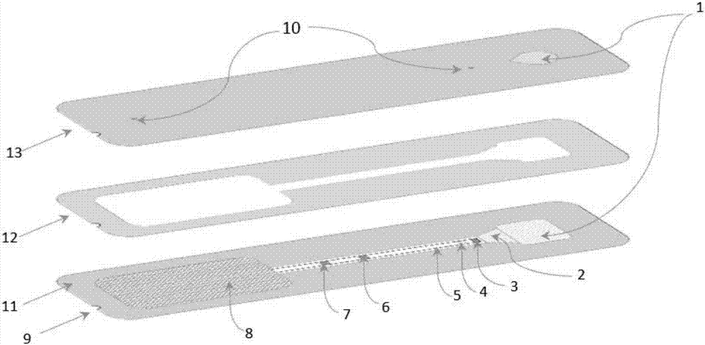
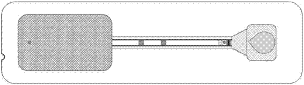
[0040] (1) The BNP microfluidic detection reagent consists of a three-layer structure, namely a cover sheet, an adhesive layer and a substrate. The cover sheet is a transparent acrylic plate (thickness 1mm), the adhesive layer is double-sided adhesive tape with a thickness of 0.115mm, and the base sheet is a non-transparent acrylic plate (thickness 2mm). The above three-layer structures are all laser engraved or cut by machine tools. The chip structure is as follows: Figure 1-2 shown.
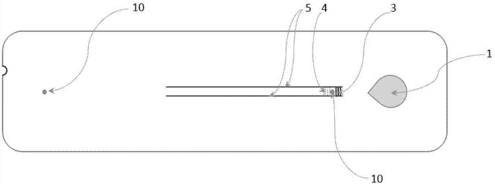
[0041] (2) Cover sheet structure such as image 3 As shown, it includes sample loading area, speed control area 1-2, exhaust hole, and microchann...
Embodiment 2
[0050] Embodiment 2, a kind of BNP microfluidic detection reagent and preparation method thereof
[0051] Except that the preparation methods of the following structural parts are different, other preparation methods are the same as in Example 1.
[0052] (1) cover sheet
[0053] a. The thickness is 0.5mm;
[0054] b. Speed control area 1: use stamping ink (Dongguan Cairong Ink Co., Ltd.) to draw 6 lines (width 1mm) (spacing 1mm);
[0055] c. Speed control area 2: Use polyether modified silicone oil (Jining Huakai Resin Co., Ltd.) to draw 6 lines (width 1mm) (spacing 1mm);
[0056] d. Microchannel control line: use polyether modified silicone oil (Jining Huakai Resin Co., Ltd.) to draw a line (width 2mm), and the distance between two microchannel control lines (microfluidic channel) is 3mm;
[0057] (3) The thickness of the substrate is 4mm, and the structure is as follows Figure 4 As shown, it includes sample loading area, speed control area 1-2, microchannel control...
Embodiment 3
[0058] Example 3, a BNP microfluidic detection chip and its preparation method
[0059] Except that the preparation methods of the following structural parts are different, other preparation methods are the same as in Example 2.
[0060] (1) The cover slip only has a sample loading area and an air vent, without the speed control area and microchannel control line in the cover slip of Example 2; the thickness of the cover slip is 2mm.
[0061] (2) The speed control area 1 of the substrate is processed by machine tools, and it is a groove with a width of 0.01mm and a depth of 0.05mm. Polyether modified silicone oil is injected into the groove, and the groove interval is 0.5mm; the thickness of the substrate is 0.5mm.
[0062] (3) The speed control area 2 of the substrate is processed by machine tools, and is a groove with a width of 0.5 mm and a depth of 0.3 mm. Marker ink is injected into the groove, and the distance between the grooves is 0.8 mm.
[0063] (4) The microchannel c...
PUM
| Property | Measurement | Unit |
|---|---|---|
| Width | aaaaa | aaaaa |
| Width | aaaaa | aaaaa |
| Thickness | aaaaa | aaaaa |
Abstract
Description
Claims
Application Information