Process for preparing high-C-axis-orientation ScAlN thin film

A film and orientation technology, which is applied in the process of preparing highly C-axis oriented ScAlN films, can solve the problems of reducing the selection range of substrate materials, high-power vacuum space, unfavorable industrial production, etc., and achieves the elimination of heating and cooling bases. The effect of slice time, energy saving, time reduction

Inactive Publication Date: 2017-07-04
UNIV OF ELECTRONICS SCI & TECH OF CHINA
View PDF0 Cites 5 Cited by
  • Summary
  • Abstract
  • Description
  • Claims
  • Application Information

AI Technical Summary

Problems solved by technology

However, most of the current processes for preparing ScAlN thin films use DC magnetron sputtering, which requires heating to a high temperature of more than 300 degrees Celsius during the preparation process. Usually, the preparation time is more than 1 hour, which has great restrictions on the substrate of the multilayer structure of the sensor device. , the preparation of piezoelectric films at high temperatures requires the substrate material to have good high temperature resistance, which greatly reduces the selection range of substrate materials. At the same time, high power and good vacuum space are required for the preparation of films. As the energy supply of the vacuum system and the sputtering source is required during the preparation of the film, the longer the preparation time of the film, the more energy it consumes, and it needs to consume huge energy in the industrial preparation process, which is not conducive to industrial production. Therefore, improving the preparation process is of great significance for the subsequent preparation of magnetic field sensors with multilayer structures.

Method used


Image

  • Process for preparing high-C-axis-orientation ScAlN thin film
  • Process for preparing high-C-axis-orientation ScAlN thin film
  • Process for preparing high-C-axis-orientation ScAlN thin film

Examples


Embodiment 1

[0030] The processing steps in the present embodiment are as follows:

[0031] Step 1: Using Si(100) as the substrate, first soak the substrate in a mixed liquid of concentrated sulfuric acid and hydrogen peroxide (liquid volume ratio H 2 SO 4 :H 2 o 2 =1:1) for 30 minutes to remove stubborn stains on the surface, then ultrasonically clean the substrate in acetone for 20 minutes, ultrasonically clean in alcohol for 10 minutes to remove surface organic pollutants, and finally use high-purity argon to dry it and place it in a sputter The ejaculation room is spare.

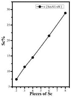
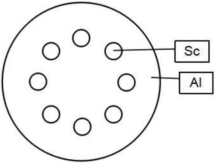
[0032] Step 2: Polish the surface of the Al target (99.999%) with a diameter of Φ=75mm and the Sc target (99.999%) with a diameter of Φ8mm until the surface is bright with 1000-mesh sandpaper, clean the surface stains with alcohol, and dry them with high-purity nitrogen. The sputtering track of the target is divided into four areas equally. One side of the 4 pieces of Sc target is coated with silver paste and pas...

Embodiment 2

[0040] The processing steps in the present embodiment are as follows:

[0041] Step 1: Si (100) is used as the substrate, and the processing method of the substrate is the same as that in the first embodiment.

[0042] Target processing:

[0043] Step 2: Al target (99.999%) and Sc target (99.999%) chip targets are used as sputtering targets, and chip target materials are implemented in the same way as in Example 1.

[0044] Step 3: Treat the Si(100) substrate in the same way as in Step 1 and grow a layer of Si on the surface of the substrate 3 N 4 layer, put the processed substrate into the PECVD instrument, and Table 2 sets the process parameters.

[0045] Table 2 Partial experimental conditions of SiN prepared by PECVD

[0046] Power / W Pressure / mT Si / Ar / sccm N2 / sccm Time / s 60 400 250 200 100

[0047] Step 4: Put the target processed in step 2 and the Si3N4 / Si substrate prepared in step 3 into the vacuum chamber. The pre-sputtering condition...


PUM

PropertyMeasurementUnit
thicknessaaaaaaaaaa
diameteraaaaaaaaaa
diameteraaaaaaaaaa

Abstract

The invention discloses a process for preparing a high-C-axis-orientation ScAlN thin film and a preparation manner for lowering the process difficulty. In the vacuum environment, N2 gas is ionized through radio frequency so that local plasmas can be generated on a substrate, and a nitride layer is formed on the substrate mentioned above through the plasmas; by means of a radio frequency magnetron sputtering manner, a Sc-doped AlN thin film is prepared and formed on the substrate with a desalination layer under the room temperature condition, and the relative molecule content of the doping amount of the element Sc in the ScAlN thin film ranges from 0% to 28.87%; and regulation and control are achieved according to requirements, the relative molecule content values of the doping amount of the element Sc in the prepared thin film include 0, 7.45%, 11.45%, 14.49%, 21.50% and 28.87%. By means of the process, orientation of the ScAlN thin film can be optimized, and meanwhile the preparation difficulty is lowered.

Description

technical field [0001] The invention relates to a preparation process for preparing a ScAlN film, that is, a process for preparing a ScAlN film with high C-axis orientation by radio frequency magnetron sputtering and its optimization. Background technique [0002] The magnetic field sensor developed by magnetoelectric composite materials has high sensitivity and small volume, adapts to the trend of miniaturized devices, and can be used in many fields such as geophysics, national defense and military, and biomedicine. A variety of sensor structures combined with magnetoelectric composite materials, surface acoustic wave technology or bulk acoustic wave technology proposed in recent years can enable the sensor to be applied to both DC and broadband AC magnetic field detection while achieving high sensitivity, which meets the application requirements. In order to obtain a magnetic field sensor with better performance. The piezoelectric film in this structure has become a resea...

Claims


Application Information

Patent Timeline
Patent Type & Authority Applications(China)
IPC IPC(8): C23C28/04C23C16/34C23C14/06C23C14/35
CPCC23C28/04C23C14/0036C23C14/0641C23C14/352C23C16/345
Inventor 杨雪梅
Owner UNIV OF ELECTRONICS SCI & TECH OF CHINA
Why Eureka
Try Eureka