Manufacturing method for source and drain region contact plug of metal gate transistor

A manufacturing method and metal gate technology, which is applied in semiconductor/solid-state device manufacturing, semiconductor devices, electric solid-state devices, etc., can solve problems such as metal gate short circuit, increase process cost, and reduce device yield, so as to reduce alignment accuracy, The effect of improving device yield and reducing lithographic fineness requirements

Active Publication Date: 2017-07-04
SEMICON MFG INT (SHANGHAI) CORP +1
View PDF2 Cites 5 Cited by
  • Summary
  • Abstract
  • Description
  • Claims
  • Application Information

AI Technical Summary

Problems solved by technology

[0004] In the prior art, in the process of making contact plugs in the source and drain regions of metal gate transistors, due to factors such as the size of the through hole, the offset between the photolithography mask and the substrate alignment stack (Overlay, OVL), the formed source and drain The area contact plug is easily shorted to the metal gate, which reduces the device yield
In order to improve the device yield, it is necessary to reduce the size of the through hole, the offset between the photolithography mask and the substrate alignment stack (Overlay, OVL), which in turn increases the process cost

Method used


Image

  • Manufacturing method for source and drain region contact plug of metal gate transistor
  • Manufacturing method for source and drain region contact plug of metal gate transistor
  • Manufacturing method for source and drain region contact plug of metal gate transistor

Examples


Embodiment Construction

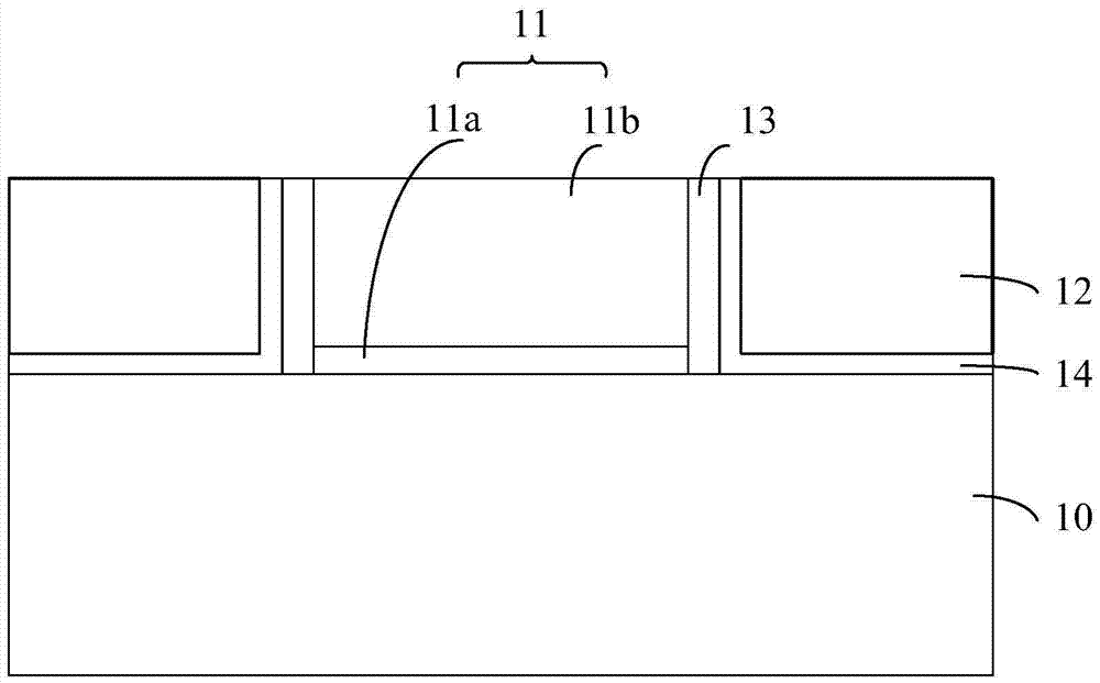
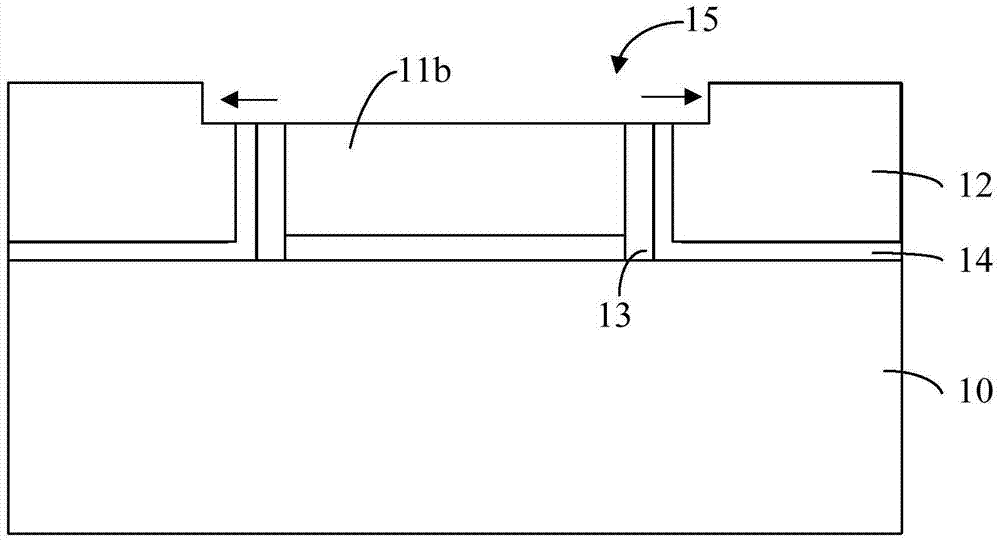
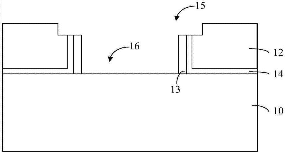
[0042] As mentioned in the background technology, in the prior art, the device yield rate in the manufacture of contact plugs in the source and drain regions of metal gate transistors is low. In order to improve the yield rate, it is necessary to improve the alignment accuracy of the mask degree, which results in higher process costs. In order to solve the above technical problems, the present invention provides a new method for manufacturing contact plugs in the source and drain regions of metal gate transistors. Specifically, an etching stopper layer with both ends wider than the metal gate structure is formed on the metal gate structure. In the process of dry etching to form the contact via hole in the source and drain regions, the etching barrier layer is used to form a protective via hole for the underlying metal gate structure and the dielectric layer, so as to prevent the via hole from exposing the metal gate, thereby avoiding the filling of the via hole. The imported c...


PUM


Abstract

Disclosed is a manufacturing method for a source and drain region contact plug of a metal gate transistor. a) for a technology of high K gate dielectric layer last and metal gate first, and in a process of removing a pseudo gate structure and filling in a high K gate dielectric layer, a work function layer and a metal gate, and b) for a technology of high K gate dielectric layer first and metal gate last, and in a process of removing a pseudo gate and filling in a work function layer and a metal gate, an etching barrier layer is formed on the metal gate structure, wherein the two ends of the etching barrier layer are both wider than the metal gate structure. By virtue of the etching barrier layer, even if alignment between a mask plate and a substrate has deviation or even if an opening, corresponding to a through hole, in the mask plate is relatively large, in a photoetching technology of forming a contact through hole in the source and drain regions in a dielectric layer subsequently, the through hole formed by etching does not expose the metal gate due to protection of the etching barrier layer on the covered metal gate structure and dielectric layer below the etching barrier layer; and therefore, a conductive materiel arranged in the through hole in a filling way is not in electrical conduction with the metal gate, so that the yield of a device is improved, the alignment precision between the mask plate and the substrate is lowered, and the requirement on the photoetching fineness is lowered.

Description

technical field [0001] The invention relates to the technical field of semiconductors, in particular to a method for manufacturing a contact plug in a source and drain region of a metal gate transistor. Background technique [0002] In semiconductor manufacturing, especially in VLSI, the main device is metal-oxide-semiconductor field-effect transistor (MOS transistor). Since the advent of MOS transistors, their geometric dimensions have been continuously reduced according to Moore's Law, but the physical limits of the devices make it increasingly difficult to scale them down. Among them, in the field of MOS transistor manufacturing, the most challenging problem is the leakage current from the gate to the substrate caused by the reduction of the thickness of the polysilicon and silicon dioxide gate dielectric layers in the process of device scaling down in the traditional MOS process. . [0003] In order to solve the above problems, in the prior art, a high-K (permittivity)...

Claims


Application Information

Patent Timeline
IPC IPC(8): H01L21/336H01L21/768
CPCH01L29/66545H01L29/66795H01L21/76895H01L2221/1068
Inventor 赵杰
Owner SEMICON MFG INT (SHANGHAI) CORP
Why Eureka
Try Eureka