Flexible resistive random access memory and preparation method

A resistive memory and flexible technology, applied in electrical components and other directions, can solve the problems of imperfect flexible memory manufacturing process and other problems, and achieve the effects of excellent flexibility, good electrical durability, and large distinction between two states.

Inactive Publication Date: 2017-07-04
GENERAL RESEARCH INSTITUTE FOR NONFERROUS METALS BEIJNG
View PDF3 Cites 3 Cited by
  • Summary
  • Abstract
  • Description
  • Claims
  • Application Information

AI Technical Summary

Problems solved by technology

Among them, the manufacturing process of the most core hardware - flexible memory (Flexible Memory) is not perfect enough

Method used


Image

  • Flexible resistive random access memory and preparation method
  • Flexible resistive random access memory and preparation method
  • Flexible resistive random access memory and preparation method

Examples


preparation example Construction

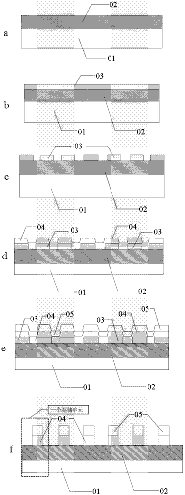
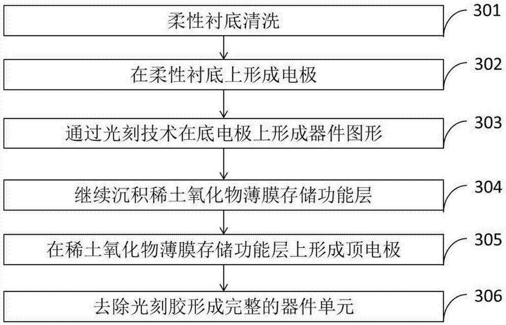
[0043] image 3 It is a flowchart of the preparation method of the flexible resistive memory of the present invention, including:

[0044] Step 301: cleaning the flexible substrate: gently wipe the surface of the substrate with alcohol, and then dry it with a nitrogen gun;

[0045] Step 302: forming an electrode on a flexible substrate: using magnetron sputtering, e-book evaporation or thermal evaporation technology to deposit a bottom electrode on the substrate;

[0046] Step 303: forming a device pattern on the bottom electrode by photolithography: using a patterning process of photolithography to form a pattern of the desired device on the bottom electrode;

[0047] Step 304: continue to deposit the rare earth oxide thin film storage function layer: use magnetron sputtering technology to deposit rare earth oxide storage function layer materials on the photoresist;

[0048] Step 305: Form a top electrode on the rare earth oxide thin film storage functional layer: use magne...

Embodiment 1

[0051] An embodiment of a method for preparing a rare earth oxide flexible resistive memory, specifically comprising the following steps:

[0052] Step 301: cleaning the substrate, gently wiping the polyethylene terephthalate (PET) with alcohol for 5 minutes, and then drying it with a nitrogen gun.

[0053] Step 302: Use magnetron sputtering technology to deposit Pt on the PET substrate to form the bottom electrode. The specific process is as follows: background vacuum 5×10 -5 Pa, working pressure 1Pa, Ar gas flow 20sccm, RF power 60W, deposition time 2min, Pt thin film 40nm.

[0054]Step 303: Use a positive photoresist to construct a memory cell pattern, use a positive mask to expose and develop the photoresist layer, retain the unexposed areas in the photoresist layer, and remove the exposed parts of the photoresist layer area, thereby defining the pattern of the device structure in the photoresist layer, and the diameter of the exposed device unit is 100 μm.

[0055] Step...


PUM


Abstract

The invention discloses a flexible resistive random access memory and a preparation method. The flexible resistive random access memory comprises a bottom electrode, a memory functional layer and a top electrode which are prepared on a flexible substrate in sequence, wherein the bottom electrode, the memory functional layer and the top electrode form a sandwich structure; and the material of the memory functional layer is rare earth oxide. The preparation method comprises the following steps of (1) forming a bottom electrode layer on the flexible substrate; (2) forming a pattern required by the memory device on the bottom electrode through a photoetching process; (3) forming a rare earth oxide thin film memory functional layer on the pattern; (4) forming a top electrode layer on the memory functional layer; and (5) removing photoresist to form a complete device unit. The flexible resistive random access memory disclosed by the invention has the advantage of maintaining memory performance stability when the flexible resistive random access memory is bent for a certain radius and bent for multiple times, so that the flexible resistive random access memory is applicable to a flexible memory technology.

Description

technical field [0001] The invention relates to a flexible resistive variable memory and a preparation method thereof, belonging to the technical field of flexible electronics. Background technique [0002] Flexible electronics technology is an emerging electronic technology that fabricates organic or inorganic material electronic devices on flexible or ductile plastic or thin metal substrates. Flexible electronic technology will bring about a revolution in electronic technology, which has attracted worldwide attention and developed rapidly. The U.S. magazine "Science" listed the development of organic electronics technology as one of the world's top ten scientific and technological achievements in 2000, alongside major discoveries such as the draft human genome and biological cloning technology. Like traditional IC technology, manufacturing process and equipment are also the main driving force for the development of flexible electronic technology. The technical level indi...

Claims


Application Information

Patent Timeline
Patent Type & Authority Applications(China)
IPC IPC(8): H01L45/00
CPCH10N70/20H10N70/826H10N70/8833H10N70/011
Inventor 赵鸿滨屠海令魏峰杨志民
Owner GENERAL RESEARCH INSTITUTE FOR NONFERROUS METALS BEIJNG
Why Eureka
Try Eureka