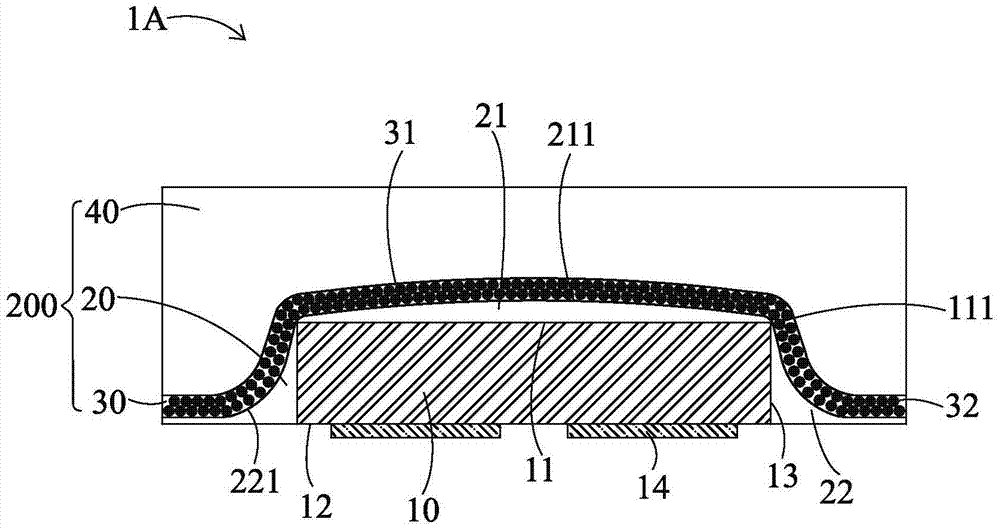
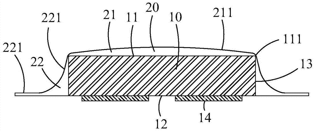
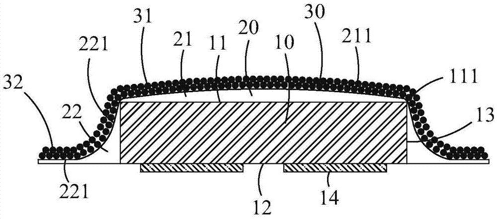
[0005] However, since the CSP light-emitting device does not require additional sub-mounts such as substrates or brackets, the fluorescent structure in the CSP light-emitting device is only in contact with the LED chip; because the contact area between the two is quite limited, it often leads to a gap between the two. Insufficient bonding force; and the
thermal expansion coefficient of the LED chip and the fluorescent structure usually has a
significant difference. Under the temperature change generated during the operation of the light emitting device, the
internal stress caused by the mismatch of the
thermal expansion coefficient will make the fluorescent structure with insufficient bonding force The structure is easy to peel off from the LED chip (
delamination), resulting in failure of the CSP light emitting device
This inherent characteristic seriously affects the reliability performance of existing CSP light emitting devices
[0006] Furthermore, during the manufacturing process of the existing CSP light-emitting device, the fluorescent material is first mixed in the binder, such as a
polymer material, and then through molding, printing or spraying ) and other methods to form fluorescent structures; when
fluorescent materials are mixed with
polymer materials, fluorescent colloids (
phosphor slurry) will be formed. When manufacturing fluorescent structures, the control of the geometric dimensions of fluorescent structures requires high precision. , in order to obtain accurate luminescent color control; and, the existing methods can only control the geometrical dimensions of the fluorescent structure, but it is difficult to control the distribution state of the fluorescent material in the fluorescent
colloid (or fluorescent structure), while the distribution state of the fluorescent material is is the key factor to determine its luminous performance
Therefore, these two innate physical properties make it difficult for
fluorescent materials to form a
conformal coating, which increases the difficulty of achieving optical consistency in
mass production of CPS light-emitting devices.
[0007] For example, when fluorescent
colloid is used for molding (or printing) the fluorescent structure of CSP light-emitting devices, the relative position between multiple LED chips (forming an LED chip array) and the inner surface of the mold (or printing scraper and steel plate) The error will cause insufficient thickness consistency of the fluorescent structure formed on the upper surface and facade of multiple LED chips; at the same time, if it is necessary to separate multiple CSP light-emitting devices by
cutting, the error in the
cutting position of the fluorescent structure will make the LED The thickness of the fluorescent structure on the chip facade is difficult to control; coupled with the inability to effectively control the distribution of the fluorescent material in the
colloid; these factors have resulted in the inability to form a
conformal coating of the fluorescent material, so that the emitted light from the LED chip After the light passes through the fluorescent structure, its color is inconsistent, resulting in poor spatial color uniformity (spatial color uniformity), and
color temperature (Correlated
Color Temperature, CCT) grading (binning) concentration is also poor, resulting in a decline in production yield
[0008] In addition, if spraying is used to make the fluorescent structure, although the related problems encountered in the alignment error of the LED chip in the molding (or printing process) can be avoided, the fluorescent material is not easy due to the effect of gravity when spraying. Attached to the vertical facade of the LED chip, the fluorescent material is not easy to form a continuous distribution on the facade, which will cause the fluorescent material to be discontinuous in the
polymer material on the facade of the LED chip, although the polymer material can be formed on the facade The transparent structure is continuously distributed, but due to the local lack of fluorescent materials, a large area of continuous optically transparent "holes" is produced, so that
blue light leaks from the holes, that is, it directly penetrates the packaging structure without
wavelength conversion by fluorescent materials, resulting in The side of the CSP light-emitting device is easy to leak
blue light, so that the color of the front light of the CSP light-emitting device is inconsistent with that of the side light to form a blue halo. Therefore, the existing spraying process cannot form a fluorescent material with a
conformal coating; When the spraying method forms a thin fluorescent structure on the upper surface of the LED chip, since the fluorescent material and the polymer material have been pre-mixed to form a fluorescent colloid, the
particle aggregation of the fluorescent material (usually granular) will make the fluorescent material Obvious distribution discontinuity appears, which will also form holes in the fluorescent material, resulting in spot (
blue light spot) phenomenon; High, in addition to causing poor spatial color uniformity, it will also increase the damage caused by blue light to human eyes; at the same time, inconsistent distribution of fluorescent materials will lead to poor
color temperature grading concentration; moreover, a large amount of blue light leakage will make fluorescent materials unable to Effective conversion of blue light wavelengths will also cause a decrease in
light conversion efficiency