


Quick Research
Generate reliable direction feasibility study reports for your R&D in just a few steps.

Technical Q&A
Discover and master advanced knowledge NOW. Basics, ideas, possibilities, all at once.

Find Solutions
As an expert in R&D theories, this can generate solutions to your technical problems instantly.

Evaluate Feasibility
Analyze your overall solution with one click, know your potential R&D risks in advance.

Monitor Landscape
Get weekly tech updates, stay abreast of the latest tech innovations and key insights.
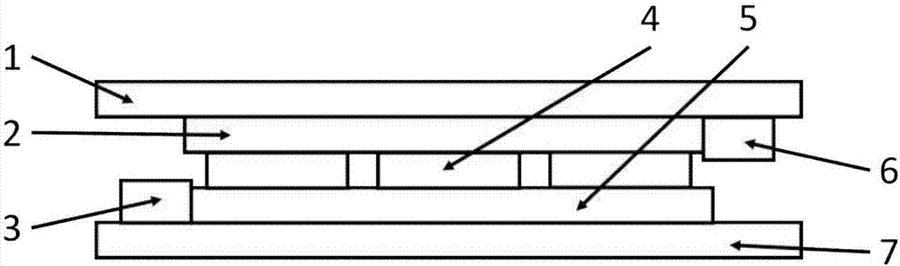
Flexible pressure sensor based on carbon nanotube film and photoresist and preparation method thereof
A carbon nanotube film and pressure sensor technology, applied in the field of flexible electronic devices, can solve the problems of unfavorable integration and large-scale production, complex manufacturing process, slow response speed, etc., and achieve easy integration and large-scale production, simple preparation method, fast response effect
- Summary
- Abstract
- Description
- Claims
- Application Information
AI Technical Summary
Problems solved by technology
Method used
Image

Examples
Embodiment 1
[0040] A kind of flexible pressure sensor based on carbon nanotube film and photoresist, its preparation method comprises the following steps:
[0041] 1) Transfer and attach a single-wall, double-wall or multi-wall carbon nanotube film (with a thickness of 20nm-2μm) on a PDMS flexible substrate with a thickness of 500μm;
[0042] 2) Deposit the silver electrode on the carbon nanotube thin film flexible electrode, so that the silver electrode covers the carbon nanotube thin film electrode edge, and reserve a large area of exposed carbon nanotube thin film electrode;
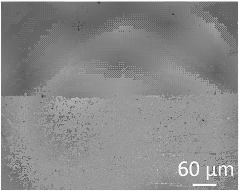
[0043] 3) The photoresist is spin-coated on the reserved carbon nanotube film electrode, and photolithography, development and glue washing are carried out to form a photoresist porous insulating layer on the carbon nanotube film electrode, wherein the thickness of the photoresist is 5μm, the diameter of the small holes is 40μm, and arranged periodically, image 3It is an optical micrograph of the photoresist ...
Embodiment 2
[0047] A kind of flexible pressure sensor based on carbon nanotube film and photoresist, its preparation method comprises the following steps:
[0048] 1) Transfer and attach a single-wall, double-wall or multi-wall carbon nanotube film (with a thickness of 20nm-2μm) on a PDMS flexible substrate with a thickness of 500μm;
[0049] 2) Deposit the silver electrode on the carbon nanotube thin film flexible electrode, so that the silver electrode covers the carbon nanotube thin film electrode edge, and reserve a large area of exposed carbon nanotube thin film electrode;
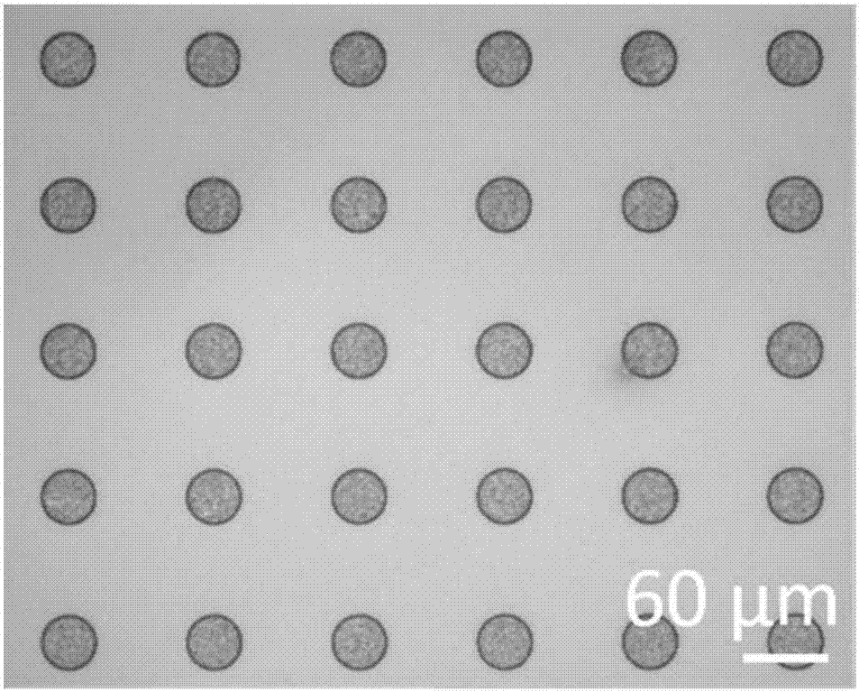
[0050] 3) The photoresist is spin-coated on the reserved carbon nanotube film electrode, and photolithography, development and glue washing are carried out to form a photoresist porous insulating layer on the carbon nanotube film electrode, wherein the thickness of the photoresist is 5μm, the diameter of the small holes is 10μm, and arranged periodically, Figure 5 It is an optical micrograph of the photoresis...
Embodiment 3
[0054] A kind of flexible pressure sensor based on carbon nanotube film and photoresist, its preparation method comprises the following steps:
[0055] 1) Transfer and attach a single-wall, double-wall or multi-wall carbon nanotube film (with a thickness of 20nm-2μm) on a PDMS flexible substrate with a thickness of 500μm;
[0056] 2) Deposit the silver electrode on the carbon nanotube thin film flexible electrode, so that the silver electrode covers the carbon nanotube thin film electrode edge, and reserve a large area of exposed carbon nanotube thin film electrode;
[0057] 3) The photoresist is spin-coated on the reserved carbon nanotube film electrode, and photolithography, development and glue washing are carried out to form a photoresist porous insulating layer on the carbon nanotube film electrode, wherein the thickness of the photoresist is 15μm, the diameter of the small holes is 20μm, and arranged periodically, Figure 7 It is an optical micrograph of the photoresi...
PUM
| Property | Measurement | Unit |
|---|---|---|
| Thickness | aaaaa | aaaaa |
| Thickness | aaaaa | aaaaa |
| Aperture | aaaaa | aaaaa |
Abstract
Description
Claims
Application Information
 - R&D Engineer
- R&D Manager
- IP Professional
- Industry Leading Data Capabilities
- Powerful AI technology
- Patent DNA Extraction
Browse by: Latest US Patents, China's latest patents, Technical Efficacy Thesaurus, Application Domain, Technology Topic, Popular Technical Reports.
© 2024 PatSnap. All rights reserved.Legal|Privacy policy|Modern Slavery Act Transparency Statement|Sitemap|About US| Contact US: help@patsnap.com