An edge-emitting semiconductor laser device and its manufacturing method

A technology of laser device and manufacturing method, applied in semiconductor lasers, laser parts, lasers, etc., can solve the problem of high laser manufacturing cost, and achieve the effects of reducing cavity surface loss, reducing manufacturing cost, and high reflectivity

Active Publication Date: 2020-06-02
GUANGDONG UNIV OF TECH
View PDF2 Cites 0 Cited by
  • Summary
  • Abstract
  • Description
  • Claims
  • Application Information

AI Technical Summary

Problems solved by technology

The production of one-dimensional photonic crystal structures on mirror surfaces requires expensive vacuum equipment, and the production of two-dimensional photonic crystals also requires electron beam lithography, holographic lithography, or nanoimprinting, which makes the manufacturing cost of lasers relatively high.

Method used


Image

  • An edge-emitting semiconductor laser device and its manufacturing method
  • An edge-emitting semiconductor laser device and its manufacturing method
  • An edge-emitting semiconductor laser device and its manufacturing method

Examples


Embodiment 1

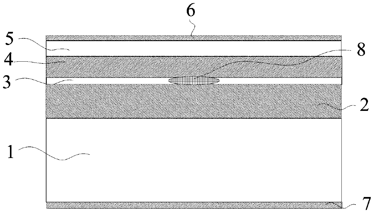
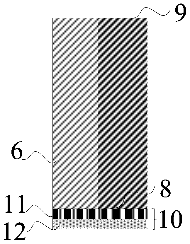
[0041] Such as figure 1 and figure 2 Shown, a kind of edge emission semiconductor laser device, it comprises substrate (1), the semiconductor epitaxial layer that is deposited on the substrate and is located at the reflective end face (8) and the exit end face (9) of semiconductor epitaxial layer surface, this semiconductor The epitaxial layer includes a first conductive coating layer (2), a light-emitting layer (3) and a second conductive coating layer (4) from bottom to top, and a second electrode (6) is arranged at one end of the second conductive coating layer (4). ), the bottom of the substrate (1) or one end of the first conductive cladding layer (2) is provided with a first electrode (7), and the reflective end surface (8) is provided with a periodic dielectric composite layer (10). Such as figure 2 As shown, the periodic dielectric composite layer (10) is composed of two parts: a three-dimensional periodically arranged dielectric layer (11) and a low refractive ind...

Embodiment 2

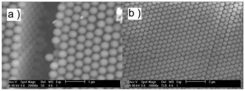
[0051] The basic structure adopted in the second embodiment is the same as that of the first embodiment, except that the shape of the three-dimensional periodically arranged dielectric layer (11) is complementary to that of the first embodiment. The key to realizing Example 2 is to fill or synthesize a certain material in the gaps of the polystyrene pellets by means of physical infiltration or chemical synthesis, and burn out the polystyrene pellets by high-temperature annealing. A specific embodiment is: SnCl4.5H2O (1.4g, 4mmol) and ethanol (20mL, 0.2M) are fully mixed. Saturated NH4F solution (0.5 g, 5 mmol) was added to the mixture and sonicated for 1 hour until the mixture was colorless. The sample obtained in Example 1 was placed in the mixed solution, placed in a vacuum box for 30 minutes and taken out. The sample was placed in a blast drying oven, the temperature was raised to 450°C at a rate of 1°C / min, and kept for 2 hours. The above process makes the precursor solu...


PUM

PropertyMeasurementUnit
thicknessaaaaaaaaaa
thicknessaaaaaaaaaa
diameteraaaaaaaaaa

Abstract

The invention discloses a side emission semiconductor laser device and a manufacturing method thereof. The laser device comprises a substrate (1), a semiconductor epitaxial layer, a reflection end face (8) and an emission end face (9). The semiconductor epitaxial layer is deposited on the substrate (1). The reflection end face and the emission end face are arranged o the side face of the semiconductor epitaxial layer. The semiconductor epitaxial layer comprises a first conductive wrapping layer (2), a light emitting layer (3) and a second conductive wrapping layer (4) from the bottom up. A second electrode (6) is arranged on one end of the second conductive wrapping layer (4). A first electrode (7) is arranged at the bottom of the substrate (1) or one end of the first conductive wrapping layer (2). A period medium composite layer (10) is arranged on the reflection end face (8) and is formed by a three-dimensional periodically arranged medium layer (11) and a low refractive index material layer (12). The invention also discloses a manufacturing method of the side emission semiconductor laser device. The laser device has high reflectivity and cavity face loss of a resonance cavity can be effectively reduced.

Description

technical field [0001] The invention relates to the field of semiconductor light-emitting devices, in particular to a structure of an edge-emitting semiconductor laser device and a manufacturing method thereof. Background technique [0002] The resonant cavity of the laser is used to provide positive feedback and control the characteristics of the oscillating beam in the cavity, which is an essential part of the laser. The resonant cavity usually consists of two planar or concave spherical mirrors perpendicular to the axis of the active medium. The resonant cavity surface of the semiconductor laser is usually formed by high vacuum coating to form a highly reflective mirror surface to obtain the excited energy required for resonance. Photonic crystal structure, as a material with photonic band gap, is widely used in the design of optoelectronic devices. The photonic crystal structure with photonic bandgap itself is a perfect reflective mirror structure, which has been appli...

Claims


Application Information

Patent Timeline
Patent Type & Authority Patents(China)
IPC IPC(8): H01S5/183H01S5/042
CPCH01S5/0425H01S5/18377
Inventor 招瑜张梦龙李京波
Owner GUANGDONG UNIV OF TECH
Why Eureka
Try Eureka