Imaging system lens group, image taking device and electronic device

A technology of imaging system and lens group, applied in the direction of optical components, optics, instruments, etc., can solve the problems of unfavorable photographic lens miniaturization, long system length, etc.

Active Publication Date: 2017-08-01
LARGAN PRECISION
View PDF5 Cites 9 Cited by
  • Summary
  • Abstract
  • Description
  • Claims
  • Application Information

AI Technical Summary

Problems solved by technology

Traditional optical systems are equipped with a large number of lenses to achieve wide viewing angle characteristics, making the total length of the system too long, which is not conducive to the miniaturization of photographic lenses

Method used


Image

  • Imaging system lens group, image taking device and electronic device
  • Imaging system lens group, image taking device and electronic device
  • Imaging system lens group, image taking device and electronic device

Examples


no. 1 example

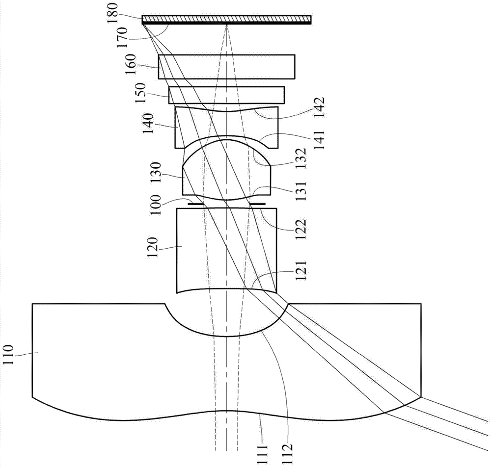
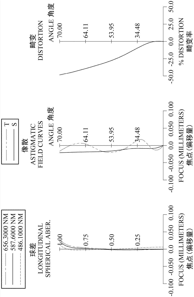
[0121] Please refer to figure 1 and figure 2 ,in figure 1 A schematic diagram of an imaging device according to a first embodiment of the present invention is shown, figure 2 From left to right are the spherical aberration, astigmatism and distortion curves of the first embodiment. Depend on figure 1 It can be known that the image capturing device includes an imaging system lens group (not another number) and an electronic photosensitive element 180 . The imaging system lens group includes a first lens 110, a second lens 120, an aperture 100, a third lens 130, a fourth lens 140, an infrared filter element (IR-cut Filter) 150, Protective glass 160 and imaging surface 170 . Wherein, the electronic photosensitive element 180 is disposed on the imaging surface 170 . There are four lenses (110-140) in the mirror group of the imaging system.

[0122] The first lens 110 has negative refractive power and is made of plastic material. Its object-side surface 111 is concave at t...

no. 2 example

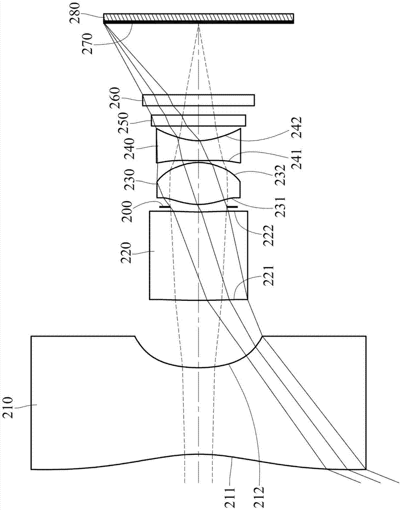
[0152] Please refer to image 3 and Figure 4 ,in image 3 A schematic diagram of an imaging device according to a second embodiment of the present invention is shown, Figure 4 From left to right are the spherical aberration, astigmatism and distortion curves of the second embodiment. Depend on image 3 It can be seen that the image capturing device includes an imaging system lens group (not another number) and an electronic photosensitive element 280 . The imaging system lens group includes the first lens 210, the second lens 220, the aperture 200, the third lens 230, the fourth lens 240, the infrared filter element 250, the protective glass 260 and the imaging surface in order from the object side to the image side. 270. Wherein, the electronic photosensitive element 280 is disposed on the imaging surface 270 . There are four lenses (210-240) in the mirror group of the imaging system.

[0153] The first lens 210 has negative refractive power and is made of plastic ma...

no. 3 example

[0165] Please refer to Figure 5 and Figure 6 ,in Figure 5 A schematic diagram of an imaging device according to a third embodiment of the present invention is shown, Figure 6 From left to right are the spherical aberration, astigmatism and distortion curves of the third embodiment. Depend on Figure 5 It can be seen that the image capturing device includes an imaging system mirror group (not another number) and an electronic photosensitive element 380 . The imaging system lens group includes the first lens 310, the second lens 320, the aperture 300, the third lens 330, the fourth lens 340, the infrared filter element 350, the protective glass 360 and the imaging surface in order from the object side to the image side. 370. Wherein, the electronic photosensitive element 380 is disposed on the imaging surface 370 . There are four lenses (310-340) in the mirror group of the imaging system.

[0166] The first lens 310 has negative refractive power and is made of plastic...


PUM


Abstract

The invention discloses an imaging system lens group, an image taking device and an electronic device. The imaging system lens group comprises a first lens, a second lens, a third lens and a fourth lens sequentially from an object side to an image side, wherein the first lens has a negative refracting power, and the surface of the image side close to the optical axis is a concave surface; the second lens has a negative refracting power; the third lens has a positive refracting power; and the fourth lens has a negative refracting power. The number of the lenses in the imaging system lens group is four. The imaging system lens group further comprises an aperture arranged between the second lens and the third lens. The invention also discloses an image taking device provided with the above imaging system lens group and an electronic device provided with the image taking device.

Description

technical field [0001] The invention relates to an imaging system mirror group, an image pickup device and an electronic device, in particular to an imaging system mirror group and an image pickup device suitable for the electronic device. Background technique [0002] In recent years, with the vigorous development of miniaturized photographic lenses, the demand for miniature imaging modules has been increasing day by day, and the photosensitive elements of general photographic lenses are nothing more than charge coupled devices (CCD) or complementary metal oxide semiconductor elements. (Complementary Metal-Oxide Semiconductor Sensor, CMOS Sensor) two types, and with the advancement of semiconductor process technology, the pixel size of the photosensitive element has been reduced, and today's electronic products are developing with good functions and thin, light and small appearance. Therefore, miniaturized photographic lenses with good imaging quality have become the mainst...

Claims


Application Information

Patent Timeline
Patent Type & Authority Applications(China)
IPC IPC(8): G02B13/00G02B13/18
CPCG02B13/0015G02B13/004
Inventor 黄歆璇杨舒雲
Owner LARGAN PRECISION
Why Eureka
Try Eureka