A flyback switching power supply
A switching power supply and flyback technology, which is applied in the direction of electrical components, adjusting electric variables, output power conversion devices, etc., can solve the problems of pin winding, small contact area, and low primary winding inductance
- Summary
- Abstract
- Description
- Claims
- Application Information
AI Technical Summary
Problems solved by technology
Method used
Image

Examples
no. 1 example
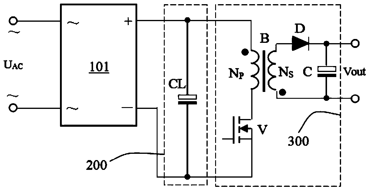
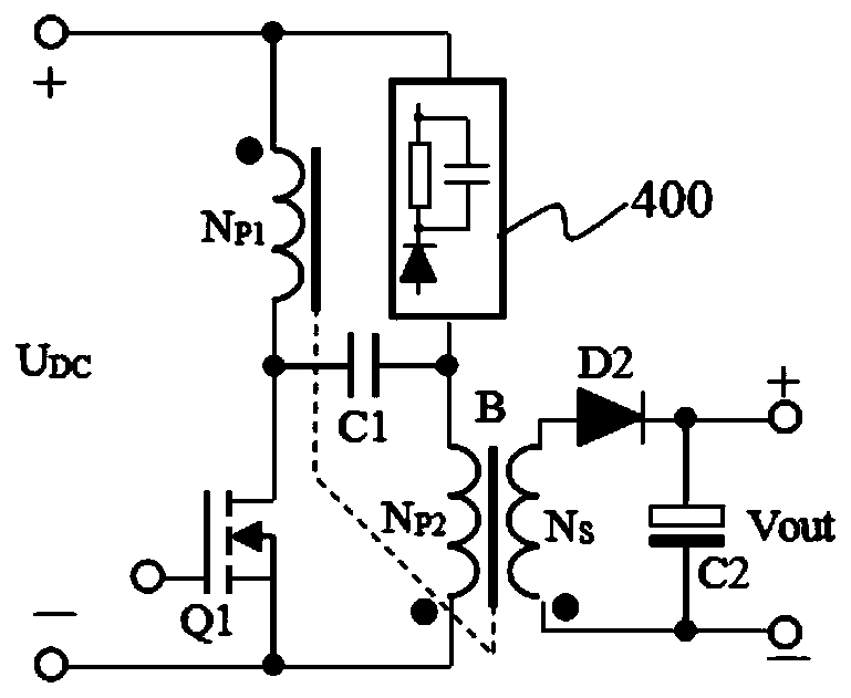
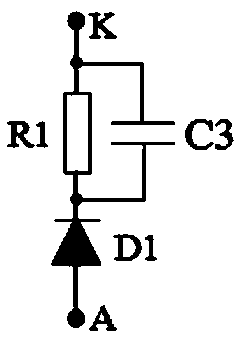
[0034] figure 2 It shows the principle diagram of the flyback switching power supply of the first embodiment of the present invention, including a transformer B, an N-channel field effect transistor Q1, a second capacitor C2, a snubber network 400, a second diode D2, and a transformer B including the first primary winding N P1 , the second primary winding N P2 and the secondary winding N S , secondary winding N S The opposite end is connected to the anode of the second diode D2, and the cathode of the second diode D2 is connected to one end of the second capacitor C2 to form a positive output, which is the + end of Vout in the figure, and the secondary winding N S The end with the same name is connected to the other end of the second capacitor C2 to form a negative output, which is the - end of Vout in the figure; the input DC power supply U DC The positive terminal + simultaneously with the first primary winding N P1 The terminal with the same name is connected to the c...
no. 2 example
[0061] The present invention also provides an equivalent solution to the above-mentioned first embodiment, corresponding to solution 2, see image 3 , a flyback switching power supply, including a transformer B, an N-channel field effect transistor Q1, a second capacitor C2, a snubber network 400, a second diode D2, and the transformer B includes a first primary winding N P1 , the second primary winding N P2 and the secondary winding N S , secondary winding N S The opposite end is connected to the anode of the second diode D2, and the cathode of the second diode D2 is connected to one end of the second capacitor C2 to form a positive output, which is the + end of Vout in the figure, and the secondary winding N S The end with the same name is connected to the other end of the second capacitor C2 to form a negative output, which is the - end of Vout in the figure; the input DC power supply U DC The positive terminal + of the N-channel field effect transistor Q1 and the second...
no. 3 example
[0078] see Figure 4 , is also the aforementioned scheme three, a flyback switching power supply, including a transformer B, a P-channel field effect transistor Q1, a second capacitor C2, a snubber network 400, a second diode D2, and the transformer B includes a first primary side winding N P1 , the second primary winding N P2 and the secondary winding N S , secondary winding N S The opposite end is connected to the anode of the second diode D2, and the cathode of the second diode D2 is connected to one end of the second capacitor C2 to form a positive output, which is the + end of Vout in the figure, and the secondary winding N S The end with the same name is connected to the other end of the second capacitor C2 to form a negative output, which is the - end of Vout in the figure; the input DC power supply U DC The negative end of - at the same time with the first primary winding N P1 The opposite end and the anode of the absorption network 400 are connected, and the firs...
PUM
 Abstract
Description
Claims
Application Information
 - R&D
- Intellectual Property
- Life Sciences
- Materials
- Tech Scout
- Unparalleled Data Quality
- Higher Quality Content
- 60% Fewer Hallucinations
Browse by: Latest US Patents, China's latest patents, Technical Efficacy Thesaurus, Application Domain, Technology Topic, Popular Technical Reports.
© 2025 PatSnap. All rights reserved.Legal|Privacy policy|Modern Slavery Act Transparency Statement|Sitemap|About US| Contact US: help@patsnap.com