Automobile glass having electric heating function and heating method thereof
A technology of automotive glass and electric heating, applied in the direction of superimposed layer plating, chemical instruments and methods, transparent/reflective heating devices, etc., can solve problems such as unexplained busbar production methods, poor film fold products, complicated processes, etc., to achieve Solve the problem of low-cost busbars, save production costs, and achieve low production costs
- Summary
- Abstract
- Description
- Claims
- Application Information
AI Technical Summary
Problems solved by technology
Method used
Image
Examples
Embodiment 1
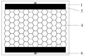
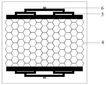
[0024] A kind of automobile glass with electric heating function, its composition includes: adhesive layer 3, metal grid 4 and connecting terminal 6, described connecting terminal is directly welded on the busbar electrode of described metal grid, and described busbar The electrodes, the metal grid and the connecting terminals constitute a metal grid conductive layer, and the bonding layer is located between the outer glass substrate 1 and the metal grid conductive layer, and the metal grid An interlayer polymer 7 is arranged between the grid conductive layer and the inner glass substrate 2, the metal grid and the busbar electrodes form a master pattern, and the conductive layer of the metal grid is sputtered with a layer by magnetron sputtering. Thin copper, then thickened to the required thickness by electroplating process.
Embodiment 2
[0026] According to the automobile glass with electric heating function described in embodiment 1, the described bonding layer is a transparent oxide, nitride or metal compound film, namely TiO2, TiN, NiCr, Si3N4, and its thickness is 20~200nm .
Embodiment 3
[0028] According to the automobile glass with electric heating function described in embodiment 1 or 2, the material of the metal grid conductive layer is Cu, Ag, Ti, Al, Ni or Zn, and the mode of magnetron sputtering is used on the bonding layer A thin film is sputtered with a thickness of 500~2000nm, and then thickened to 10~30μm by electroplating.
PUM
| Property | Measurement | Unit |
|---|---|---|
| Thickness | aaaaa | aaaaa |
| Thickness | aaaaa | aaaaa |
| Line width | aaaaa | aaaaa |
Abstract
Description
Claims
Application Information


