Miniaturized blue light laser device for semiconductor laser direct frequency doubling
A laser direct, semiconductor technology, applied in semiconductor lasers, lasers, devices for controlling laser output parameters, etc., can solve the problems of low cost performance, complex system, high price, etc., and achieve high optical conversion efficiency, small size, and low implementation cost. Effect
- Summary
- Abstract
- Description
- Claims
- Application Information
AI Technical Summary
Problems solved by technology
Method used
Image

Examples
Embodiment 1
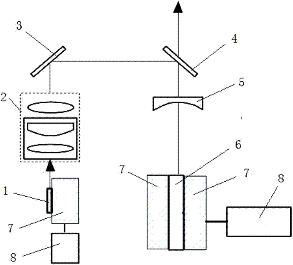
[0054] Such as figure 1 As shown, a miniaturized blue laser with direct frequency doubling of a semiconductor laser includes a near-infrared semiconductor laser 1, a beam shaping and coupling lens group 2, a beam reflection device, a PPLN crystal, a heat sink 7 and a temperature controller 8. The beam The shaping and coupling lens group 2 is placed on the emitting end side of the near-infrared semiconductor laser 1. Both sides of the beam shaping and coupling lens group 2 are coated with a near-infrared laser antireflection coating. The laser beam is coupled by the beam shaping and coupling lens group 2. To the PPLN crystal in the optical oscillation cavity, both ends of the PPLN crystal 6 are equipped with optical oscillation cavities, and the PPLN crystal 6 is placed at the light waist position of the optical oscillation cavity, and the blue laser output is formed after oscillation in the optical oscillation cavity. The heat sink 7 is set There are three, respectively connecte...
Embodiment 2
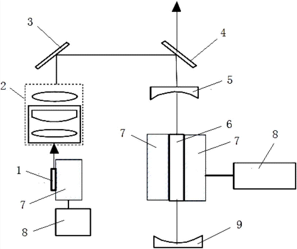
[0063] Such as figure 2 As shown, a miniaturized blue laser with direct frequency doubling of a semiconductor laser includes a near-infrared semiconductor laser 1, a beam shaping and coupling lens group 2, a beam reflection device, a PPLN crystal, a heat sink 7 and a temperature controller 8. The beam The shaping and coupling lens group 2 is placed on the side of the emitting end of the near-infrared semiconductor laser 1. Both sides of the beam shaping and coupling lens group 2 are coated with a near-infrared laser high-transmitting film. The beam is shaped and the coupling lens group 2 and the beam After the reflection device is coupled to the PPLN crystal in the optical oscillation cavity, both ends of the PPLN crystal 6 are equipped with optical oscillation cavities, and the PPLN crystal 6 is placed at the light waist position of the optical oscillation cavity, and the blue laser output is formed after oscillation in the optical oscillation cavity. There are three heat sink...
Embodiment 3
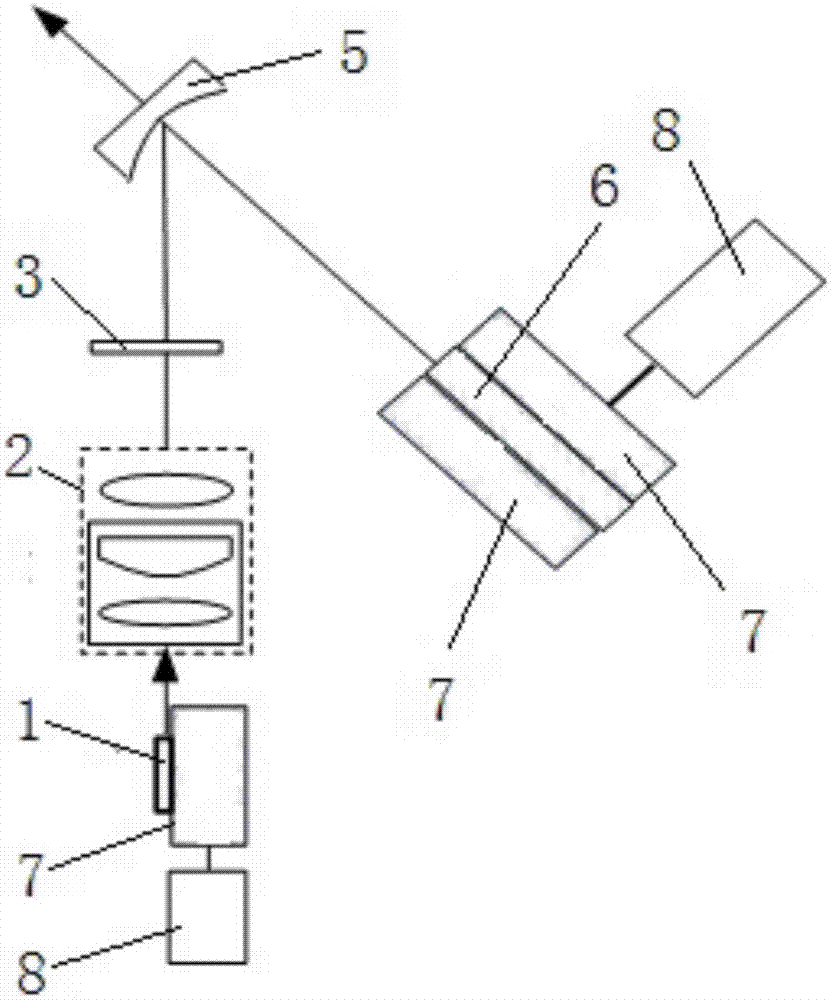
[0073] Such as image 3 As shown, a miniaturized blue laser with direct frequency doubling of a semiconductor laser includes a near-infrared semiconductor laser 1, a beam shaping and coupling lens group 2, a beam reflection device, a PPLN crystal, a heat sink 7 and a temperature controller 8. The beam The shaping and coupling lens group 2 is placed on the side of the emitting end of the near-infrared semiconductor laser 1. Both sides of the beam shaping and coupling lens group 2 are coated with a near-infrared laser antireflection coating. The beam is coupled to the near-infrared laser through the beam shaping and coupling lens group 2. The PPLN crystal in the optical oscillation cavity, the two ends of the PPLN crystal 6 are equipped with optical oscillation cavities, the PPLN crystal 6 is placed in the optical waist position of the optical oscillation cavity, and the blue laser output is formed after oscillation in the optical oscillation cavity. The heat sink 7 is equipped wit...
PUM
 Abstract
Description
Claims
Application Information
 - R&D Engineer
- R&D Manager
- IP Professional
- Industry Leading Data Capabilities
- Powerful AI technology
- Patent DNA Extraction
Browse by: Latest US Patents, China's latest patents, Technical Efficacy Thesaurus, Application Domain, Technology Topic.
© 2024 PatSnap. All rights reserved.Legal|Privacy policy|Modern Slavery Act Transparency Statement|Sitemap