Infrared metamaterial absorber and preparation method therefor

A technology of material absorption and infrared ultrasonography, applied in the field of infrared detection, can solve the problems of low signal response efficiency, achieve the effects of easy fabrication and arrangement, simplified process, and perfect absorption effect

Inactive Publication Date: 2017-09-08
UNIV OF ELECTRONICS SCI & TECH OF CHINA +1
View PDF4 Cites 10 Cited by
  • Summary
  • Abstract
  • Description
  • Claims
  • Application Information

AI Technical Summary

Problems solved by technology

However, the signal response efficiency of traditional double-sided band detectors is very low due to the existence of complex material components and surface structures

Method used


Image

  • Infrared metamaterial absorber and preparation method therefor
  • Infrared metamaterial absorber and preparation method therefor

Examples


preparation example Construction

[0047] Its preparation method comprises the following steps:

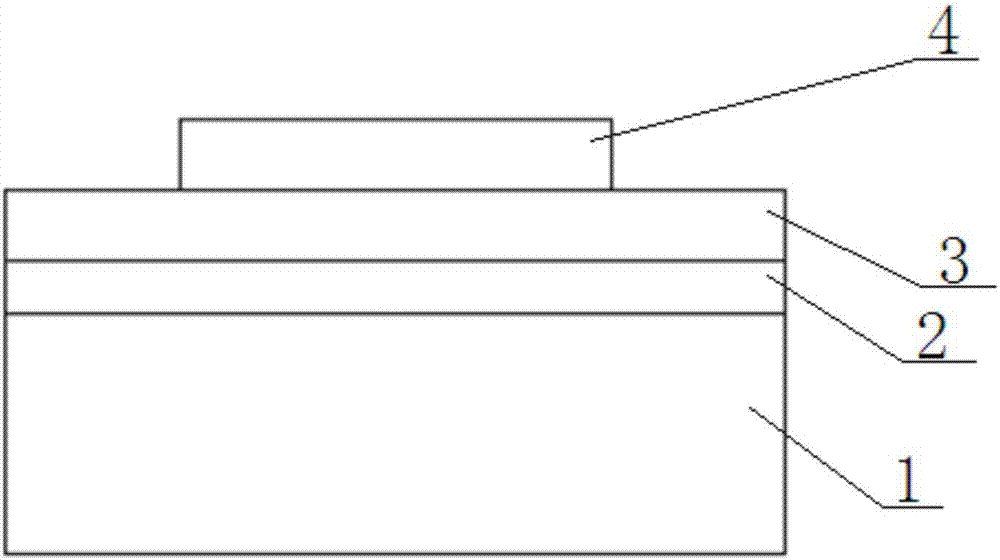
[0048] (1) Provide a base 1, the material of the base 1 is silicon or gallium arsenide;

[0049] (2) grow thin film layer 2 on described substrate 1, the material of described thin film layer 2 is any one in gold, silver, copper aluminum, thickness is not more than 200nm, adopts electron beam evaporation or magnetron sputtering method to form ;

[0050](3) Growing a dielectric layer 3 on the thin film layer 2, the material of the dielectric layer 3 is any one of silicon nitride, silicon oxide, aluminum oxide, and magnesium fluoride, and the thickness is not more than 300nm. Formation by any one of evaporation, magnetron sputtering, atomic layer deposition, and plasma enhanced chemical vapor deposition;

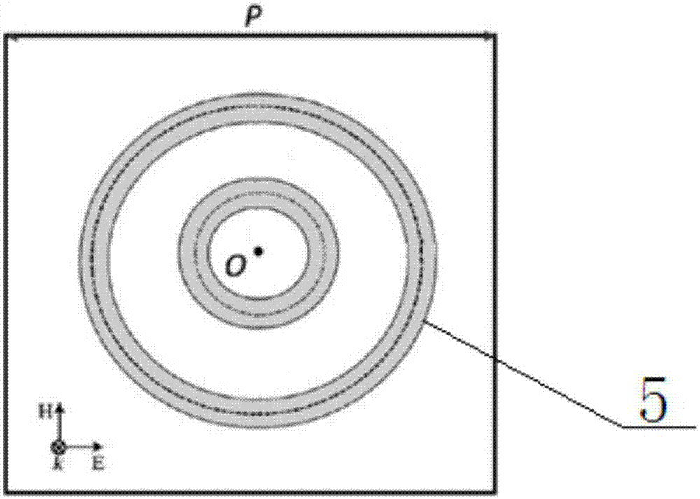
[0051] (4) Form a resonant ring structure layer 4 on the dielectric layer 3, the resonant ring structure layer 4 includes at least one metal nano-ring 5, the radius of the metal nano-ring 5 is not more than 2000n...

Embodiment 1

[0055] Such as figure 1 , figure 2 As shown, an infrared metamaterial absorber described in this embodiment includes a substrate 1, a film layer 2, a dielectric layer 3, and a resonant ring structure layer 4 arranged in sequence, and the resonant ring structure layer 4 includes at least one metal nanometer Ring 5.

[0056] Its specific preparation method is as follows:

[0057] (1) Provide a base 1, the material of the base 1 is silicon or gallium arsenide;

[0058] (2) growing a thin film layer 2 on the substrate 1, which is formed by electron beam evaporation or magnetron sputtering;

[0059] (3) growing a dielectric layer 3 on the thin film layer 2, using any one of electron beam evaporation, magnetron sputtering, atomic layer deposition, and plasma enhanced chemical vapor deposition;

[0060] (4) Forming a resonant ring structure layer 4 on the dielectric layer 3, the resonant ring structure layer 4 includes at least one metal nanoring 5, adopts deep ultraviolet litho...

Embodiment 2

[0063] According to Embodiment 1, an infrared metamaterial absorber described in this embodiment, the substrate 1 is made of p-type doped silicon, the thin film layer 2 is made of gold, and the thickness is 100nm; the dielectric layer 3 is made of silicon oxide. , thickness is 250nm; the quantity of metal nanoring 5 is 1, adopts gold as material, and thickness is 100nm, and the radius of metal nanoring 5 is 450nm, and width is 100nm; Period P is 2400nm, adopts the preparation method described in embodiment 1 Prepare to become a finished product. With this embodiment, total absorption of waves around 4300 nm in the mid-infrared can be achieved.


PUM

PropertyMeasurementUnit
radiusaaaaaaaaaa
widthaaaaaaaaaa
thicknessaaaaaaaaaa

Abstract

The invention discloses an infrared metamaterial absorber. The metamaterial absorber comprises a substrate, a thin film layer, a dielectric layer and a resonance ring structural layer which are arranged in sequence; the resonance ring structural layer comprises at least one metal nanometer ring; the radius of the metal nanometer ring is not greater than 2,000nm; and the width of the metal nanometer ring is not greater than 100nm. The infrared metamaterial absorber can be applied to infrared detection, so that dual-peak or multi-peak absorption of different infrared wavebands can be realized, and the absorptivity can be improved to be 98% or above.

Description

technical field [0001] The invention relates to the field of infrared detection, in particular to an infrared metamaterial absorber and a preparation method thereof. Background technique [0002] Absorbers of mid- and far-infrared can be used to manufacture infrared detectors, which have a wide range of applications in biosensing, thermal imaging, and medical diagnosis. Traditional infrared detection materials require a low-temperature environment, which is not only high in cost, but also sacrifices their convenience; detector materials in groups IV-VI have been widely studied, but their mechanical properties are poor and their dielectric constants are large; III-V The materials of the elements of the group have a very mature technology and can be made into a monolithic integrated circuit, but they will form a lattice mismatch when forming a heterogeneous epitaxy; quantum dots and quantum wells are also used in photodetectors , but the weak absorption of quantum dots at roo...

Claims


Application Information

Patent Timeline
Patent Type & Authority Applications(China)
IPC IPC(8): H01L31/09H01L31/02H01L31/18
CPCH01L31/02H01L31/09H01L31/18Y02P70/50
Inventor 王志明余鹏姚依森巫江刘德胜姬海宁牛晓滨
Owner UNIV OF ELECTRONICS SCI & TECH OF CHINA
Why Eureka
Try Eureka