Electrostatic chuck device

An electrostatic chuck and electrode layer technology, which is applied in the manufacture of circuits, electrical components, semiconductor/solid-state devices, etc. The effect of improving the electric constant, avoiding technical barriers, and uniform electrostatic adsorption force

Inactive Publication Date: 2017-09-12
BEIJING U PRECISION TECH
View PDF4 Cites 3 Cited by
  • Summary
  • Abstract
  • Description
  • Claims
  • Application Information

AI Technical Summary

Problems solved by technology

When this kind of electrostatic chuck is in use, its corrosion resistance is poor, and it is easy to cause a decrease in electrostatic adsorption force and a decrease in the life of the electrostatic chuck, uneven electrostatic adsorption force, and high requirements for equipment in the manufacturing process.

Method used


Image

  • Electrostatic chuck device
  • Electrostatic chuck device

Examples


Embodiment Construction

[0015] In order to make the technical problems, technical solutions and advantages to be solved by the present invention clearer, the following will describe in detail with reference to the drawings and specific embodiments.

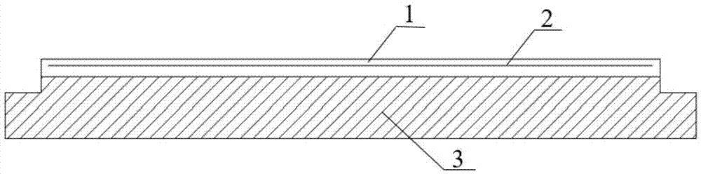
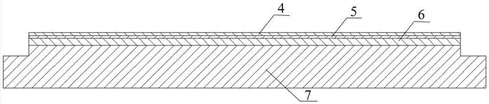
[0016] The invention provides an electrostatic chuck device, such as figure 2 As shown, it includes a first insulating layer 4, a second insulating layer 6, an electrode layer 5 and a metal layer 7, the first insulating layer 4 is arranged above the second insulating layer 6, and the electrode layer 5 is arranged on the first insulating layer 4 and the metal layer 7. Between the second insulating layers 6 , the second insulating layer 6 is disposed on the metal layer 7 , and the first insulating layer is made of sapphire material.

[0017] The inventors have discovered through research that the metal base is connected to an RF bias, and used as a cold sink or a heat source to control the temperature of the wafer. Generally, the insulating layer is usua...


PUM


Abstract

The invention discloses an electrostatic chuck device and belongs to the technical field of semiconductor wafer processing. The electrostatic chuck comprises a first insulation layer, a second insulation layer, an electrode layer and a metal layer. The first insulation layer is arranged above the second insulation layer. The electrode layer is arranged between the first insulation layer and the second insulation layer. The second insulation layer is arranged on the metal layer. The first insulation layer is of sapphire material. The electrostatic chuck device has strong anti-corrosion capability and uniform electrostatic absorption capacity, and has low requirements for equipment.

Description

technical field [0001] The invention relates to a semiconductor wafer processing device, in particular to an electrostatic chuck device. Background technique [0002] In the integrated circuit (IC) manufacturing process, especially in etching (ETCH), physical vapor deposition (PVD) and chemical vapor deposition (CVD), in order to fix and support the wafer to avoid movement or dislocation of the wafer during processing , often use chucks or suction cups to fix and support the wafer. Commonly used chucks or suction cups include mechanical chucks, vacuum chucks and electrostatic chucks (ESC: Electro Static Chuck for short). [0003] The mechanical chuck fixes and supports the wafer through the mechanical arm. The disadvantage is that the mechanical chuck is easy to cause damage to the wafer due to pressure, collision, etc.; the movement of the mechanical chuck in the reaction chamber is easy to generate particles and cause pollution to the wafer; at the same time When the mec...

Claims


Application Information

Patent Timeline
Patent Type & Authority Applications(China)
IPC IPC(8): H01L21/683
CPCH01L21/683H01L21/6831H01L21/6833
Inventor 朱煜徐登峰许岩杨鹏远穆海华成荣唐娜娜韩玮琦张鸣杨开明
Owner BEIJING U PRECISION TECH
Why Eureka
Try Eureka