
Layered electroforming method for slotted rectangular waveguides
A rectangular waveguide and electroforming technology, which is used in electroforming and electrolysis processes to achieve the effects of strong process adaptability, improved processing efficiency and reduced processing time.
- Summary
- Abstract
- Description
- Claims
- Application Information
AI Technical Summary
Problems solved by technology
Method used
Image

Examples
Embodiment Construction
[0028] The slotted rectangular waveguide that needs to be prepared is as Figure 10 As shown, the following preparation process is adopted:
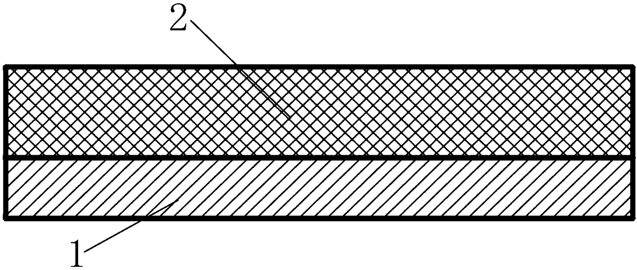
[0029] Step 1: coating a layer of photoresist 2 with a thickness of L1 on the surface of the substrate 1;
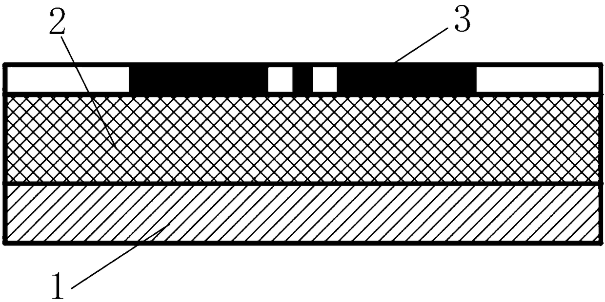
[0030] Step 2: Place the substrate 1 that has been coated for the first time in step 1 on the stage of the lithography machine, and use the first exposure mask 3 to perform the first exposure;
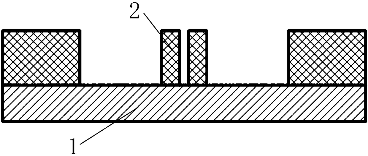
[0031] Step 3: Put the substrate 1 after the first exposure in step 2 into the developing solution for the first development, wash and dry after development;
[0032] Step 4: Electroform a layer of thickness L1 on the surface of the substrate 1 after the first development in step 3
[0033] Copper 4;
[0034] Step 5: Perform precision polishing on the surface of the electroformed copper 4 in step 4 to ensure that the thickness of the first layer of copper 4 is L2;
[0035] Step 6: Coating a layer of photolithography with a thickness of ...
PUM
| Property | Measurement | Unit |
|---|---|---|
| surface roughness | aaaaa | aaaaa |
Abstract
Description
Claims
Application Information