

Manufacturing method of enhanced P type gate GaN HEMT device
A manufacturing method and enhanced technology, applied in semiconductor/solid-state device manufacturing, semiconductor devices, electrical components, etc., can solve the problems of high difficulty and inconspicuous realization, and achieve reduced current collapse, stable chemical properties, and process compatibility high effect
- Summary
- Abstract
- Description
- Claims
- Application Information
AI Technical Summary
Problems solved by technology
Method used
Image

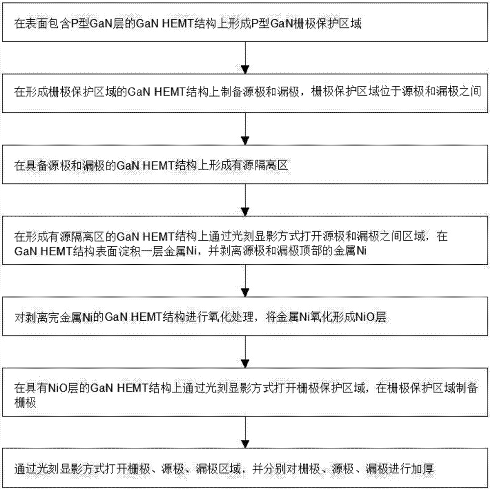
Examples
Embodiment Construction
[0026] In order to make the purpose, technical solution and advantages of the present application clearer, the present application will be further described in detail below in conjunction with the accompanying drawings and specific embodiments. For simplicity, some technical features known to those skilled in the art are omitted from the following description.
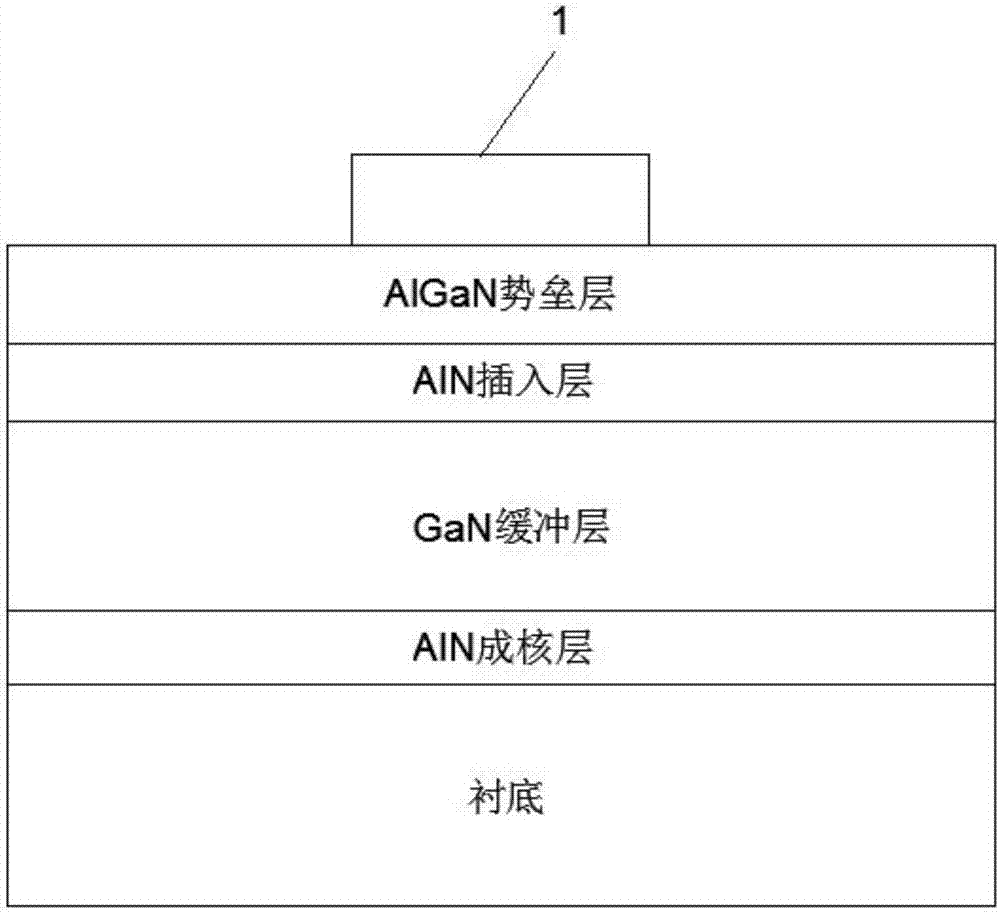
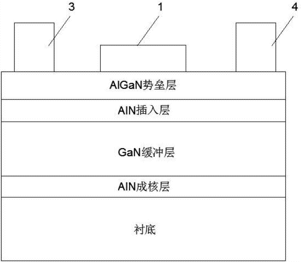
[0027] like figure 1 As shown, the GaN HEMT structure of this embodiment includes a substrate, an AlN nucleation layer, a GaN buffer layer, an AlN insertion layer, and an AlGaN barrier layer from bottom to top. There is a P-type GaN layer on the AlGaN barrier layer. The manufacturing method of the P-type gate GaN HEMT device comprises the following steps:
[0028] S1. Form a P-type GaN gate protection region 1 on the GaN HEMT structure with a P-type GaN layer on the surface, such as figure 2 shown;
[0029] Step S1 is specifically: using AZ5214 photoresist as a protective mask, forming a protective mask of the gate...
PUM
 Abstract
Description
Claims
Application Information