tft array substrate structure

An array substrate structure and array technology, applied in semiconductor devices, electrical components, circuits, etc., can solve problems such as poor contact, affecting the yield and reliability of TFT array substrates, ITO climbing and breaking, and achieve reliable connection, Improvement of yield rate and reliability, prevention of breakage and poor contact

Active Publication Date: 2020-05-29
TCL CHINA STAR OPTOELECTRONICS TECH CO LTD
View PDF5 Cites 0 Cited by
  • Summary
  • Abstract
  • Description
  • Claims
  • Application Information

AI Technical Summary

Problems solved by technology

This existing TFT array substrate adopts dry etching with both chemical etching and physical etching when making the integrated through hole V1' and common via hole V2', which is located under the drain D3 of the discharge TFT T3 The semiconductor active layer 400 and the gate insulating layer 200 are etched in dry etching gas sulfur hexafluoride (SF 6 ) under the action of a chemical reaction to form gas volatilization, and because the semiconductor active layer 400 (the material composition is amorphous silicon (a-Si) and N-type heavily doped amorphous silicon (N+a-Si)) and The material composition of the gate insulating layer 200 (the material composition is silicon nitride (SiNx)) is different from that of SF 6 In addition, the metal cross-section of the drain D3 of the discharge TFT T3 and the cross-section of the semiconductor active layer 400 are exposed by the through hole V1' and the common via V2', resulting in a gap between the drain D3 of the TFT T3 and the semiconductor active layer 400. The interface of the source layer 400 and the interface of the semiconductor active layer 400 and the gate insulating layer 200 are formed as follows: image 3 The undercut problem shown (circled by a dotted ellipse) is likely to cause the risk of fracture and poor contact of the ITO climbing slope, affecting the yield and reliability of the TFT array substrate

Method used


Image

  • tft array substrate structure
  • tft array substrate structure
  • tft array substrate structure

Examples


Embodiment Construction

[0027] In order to further illustrate the technical means adopted by the present invention and its effects, the following describes in detail in conjunction with preferred embodiments of the present invention and accompanying drawings.

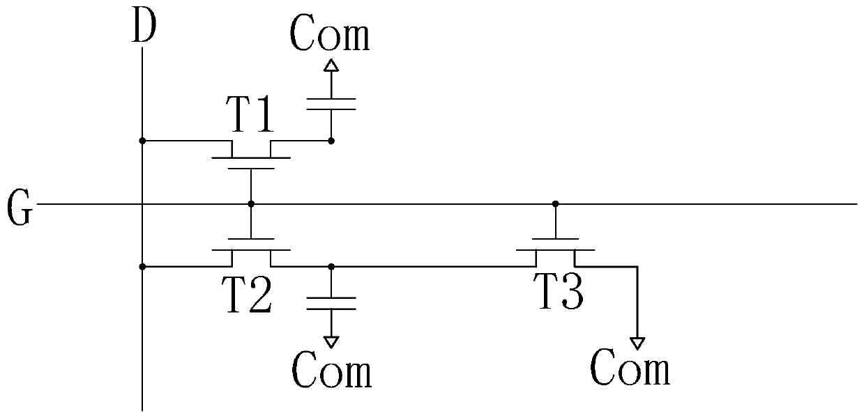
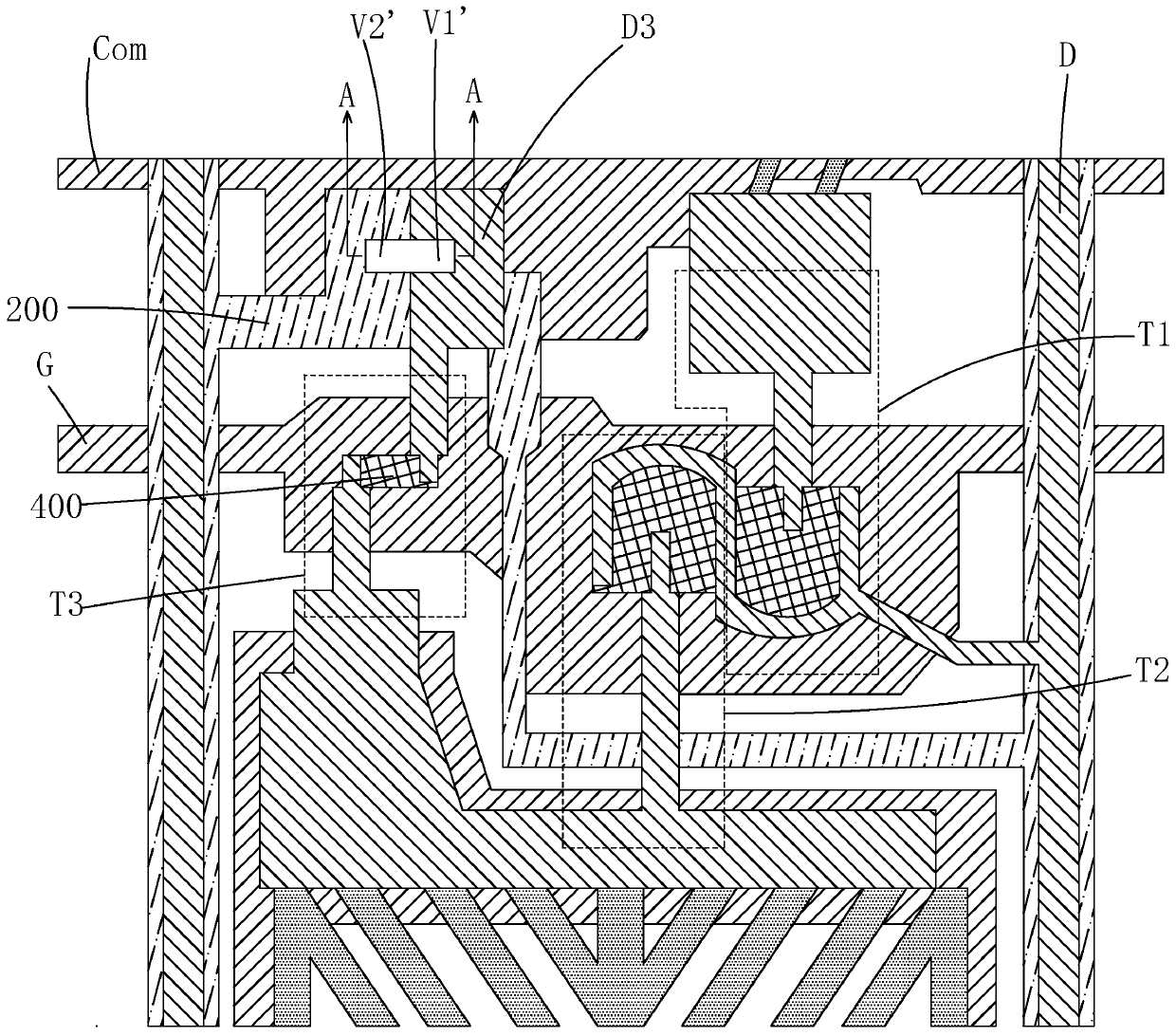
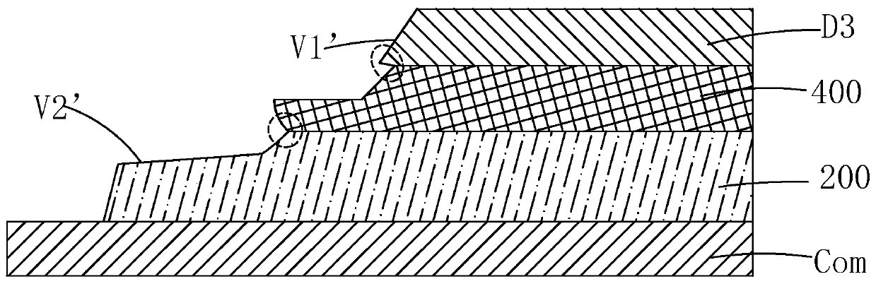
[0028] Please also see Figure 4 and Figure 5 The present invention provides a TFT array substrate structure, including a first metal layer, a gate insulating layer 3 , a semiconductor active layer 5 , a second metal layer, and a passivation insulating layer 8 stacked in sequence from bottom to top.

[0029] The TFT array substrate structure has a plurality of pixel areas arranged in an array, and in two vertically adjacent pixel areas, the first metal layer includes a common voltage line Com and a gate line G extending laterally, The second metal layer includes a data line D extending longitudinally, a first source S1 connected to the data line D, a second source S2 connected to the data line D, and a first source S2 connected to the first ...


PUM


Abstract

The invention provides a TFT (thin film transistor) array substrate structure. A first through hole (V1) is formed in a passivation insulation layer (8), a second through hole (V2) is formed in the passivation insulation layer (8) and a gate insulation layer (3), the first through hole (V1) and the second through hole (V2) are formed at an interval in the horizontal direction, and a conductive thin film (9) for connecting a third drain (D3) and a common voltage line (Com) is deposited in the first through hole (V1) and the second through hole (V2) as well as between the first through hole (V1) and the second through hole (V2). Chamfering can be avoided, risks of breakage and poor contact of the conductive thin film are prevented, connection between a discharge TFT and the common voltage line is reliable, and the yield and the reliability of a TFT array substrate are improved.

Description

technical field [0001] The present invention relates to the field of display technology, in particular to a TFT array substrate structure. Background technique [0002] Thin Film Transistor Liquid Crystal Display (TFT-LCD) can display high-definition, continuous, and delicate images, and is more and more popular among consumers. [0003] The existing TFT-LCDs on the market generally include a housing, a liquid crystal panel disposed in the housing, and a backlight module disposed in the housing. The liquid crystal panel is composed of a color filter (Color Filter, CF) substrate, a thin film transistor array substrate (ThinFilm Transistor Array Substrate, TFT Array Substrate), and a liquid crystal layer (Liquid Crystal Layer) arranged between the two substrates. The working principle is to control the rotation of the liquid crystal molecules in the liquid crystal layer by applying a driving voltage on the two glass substrates, and refract the light from the backlight module ...

Claims


Application Information

Patent Timeline
Patent Type & Authority Patents(China)
IPC IPC(8): H01L27/12
CPCH01L27/124H01L27/1248H01L27/127
Inventor 磨光阳
Owner TCL CHINA STAR OPTOELECTRONICS TECH CO LTD
Why Eureka
Try Eureka