
Pixel driving unit, forming method thereof, display panel and pixel driving circuit

A driving unit and pixel technology, applied in circuits, electrical components, electrical solid-state devices, etc., can solve problems such as poor uniformity of LTPSTFT devices, affecting display brightness stability, and large differences in driving current, achieving low cost and high integration degree, the effect of reducing the area

Active Publication Date: 2017-10-13
SHANGHAI JIAO TONG UNIV
View PDF8 Cites 17 Cited by
  • Summary
  • Abstract
  • Description
  • Claims
  • Application Information

AI Technical Summary

Problems solved by technology

However, the polycrystalline structure of the active layer in the LTPS TFT device leads to poor uniformity of the LTPS TFT device itself. The threshold voltage of each LTPS TFT is different. When working near the sub-threshold, the driving current provided under the same bias voltage is too different Big
For AOS TFT, due to the poor bias voltage and environmental stability of AOSTFT, the threshold voltage will drift after driving OLED for a long time, especially when working near the sub-threshold, the slight drift of the threshold voltage will cause the driving current to change significantly. Affects the stability of the final display brightness
[0007] The existing technology can improve the stability of the display brightness by adding an additional compensation circuit in the circuit, but all the current schemes of the compensation circuit in the pixel are based on the working range above the threshold voltage. When the thin film transistor works in the sub-threshold region, will not be able to effectively compensate
[0008] Therefore, the performance of the existing pixel driving circuit needs to be further improved

Method used


Image

  • Pixel driving unit, forming method thereof, display panel and pixel driving circuit
  • Pixel driving unit, forming method thereof, display panel and pixel driving circuit
  • Pixel driving unit, forming method thereof, display panel and pixel driving circuit

Examples


Embodiment Construction

[0038] The specific embodiments of the pixel driving unit and its forming method, the display backplane, and the pixel driving circuit provided by the present invention will be described in detail below with reference to the accompanying drawings.

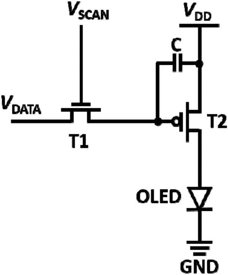
[0039] Please refer to Figure 1A , Is a schematic diagram of an equivalent circuit of a pixel driving circuit according to an embodiment of the present invention.

[0040] The pixel driving circuit includes: a second transistor T2, the second transistor T2 is an organic thin film transistor; a first transistor T1, the first transistor T1 is a low temperature polysilicon thin film transistor or an amorphous oxide thin film transistor, the first transistor T1 The gate of a transistor T1 is connected to the scan signal terminal V SCAN , The drain electrode of the first transistor T1 is connected to the data signal terminal V DATA , The source electrode of the first transistor T1 is connected to the gate of the second transistor T2; the f...


PUM


Abstract

The invention relates to a pixel driving unit, a forming method thereof, a display panel and a pixel driving circuit. The pixel driving unit includes a substrate, a second active layer, a second source electrode and a second drain electrode; a first transistor is arranged in the substrate; the first transistor is a low-temperature polysilicon thin film transistor or an amorphous oxide thin film transistor and comprises a first gate electrode, a first source electrode and a first drain electrode, wherein the surfaces of the first source electrode and the first drain electrode are provided with an insulating layer; the second active layer is located on the surface of the insulating layer; the second source electrode and the second drain electrode are located at two sides of the second active layer respectively; the projections of the second source electrode and the second active layer on the surface of the substrate overlap with the projection of the first source electrode on the surface of the substrate, so that portions of the first source electrode, the insulating layer, the second active layer, the second drain electrode and the second source electrode form a second transistor; the second transistor is an organic thin film transistor; and portions of the first source electrode, the second source electrode and the insulating layer form a first capacitor. The pixel driving unit is high in integration degree and is stable in performance.

Description

Technical field [0001] The present invention relates to the field of display technology, and in particular to a pixel driving unit and a forming method thereof, a display backplane, and a pixel driving circuit. Background technique [0002] Generally speaking, in an active matrix display device, an image is displayed by a large number of pixel circuits. Each individual pixel circuit includes a light emitting device and a driving circuit. Compared with a voltage-driven liquid crystal display, a display device using a current-driven organic electroluminescence element does not require a backlight, has a faster response speed, and can present a more realistic display effect. In the pixel circuit, the active unit in each driving circuit controls the current flowing through the OLED element to adjust the brightness. The active cell includes at least a switching transistor, a driving transistor, a capacitor, and an OLED element to form a complete pixel circuit, where the switching tr...

Claims


Application Information

Patent Timeline
IPC IPC(8): G09G3/3225H01L27/32
CPCG09G3/3225H10K59/1213H10K59/1216H10K59/125
Inventor 郭小军赵家庆刘文江樊嘉丽许兴华
Owner SHANGHAI JIAO TONG UNIV
Features
  • Generate Ideas
  • Intellectual Property
  • Life Sciences
  • Materials
  • Tech Scout
  • Unparalleled Data Quality
  • Higher Quality Content
  • 60% Fewer Hallucinations
Learn More